Instruction Decoder and Sequencer (IDS)The following block diagram illustrates the idea of our hardwired Instruction Decoder and Sequencer (IDS) but first, lets establish the following:
1.- The op. cod. is 8-bits wide and does not contain bit-mapped fields; it is basically an "instruction number".
2.- Instruction cero is not a real instruction but the number for the Op Cod Fetch cycle. Therefore we have room for a maximum of 255 instructions.
3.- Op Cod Fetch cycle takes 3 periods (T1, T2 and T3).
4.- Execution takes 1 to 9 clock periods, depending on the instruction. If more than one machine cycle are involved (for instance, an instruction with operands) we count its periods consecutively without breaking between machine cycles. For example, the instruction "LD A, addr". (load register A from memory location at address "addr") will be fetched during T1, T2, T3 and then executed during T1, T2, T3 (addr LSB operand), T4, T5, T6 (addr MSB operand), T7, T8, T9 (actual execution).
5.- Most instructions will exectute in two or three clock cycles. Only instructions with two-bytes operands will takes the longest exectuion time (9 clock cycles).
Now, the diagram.
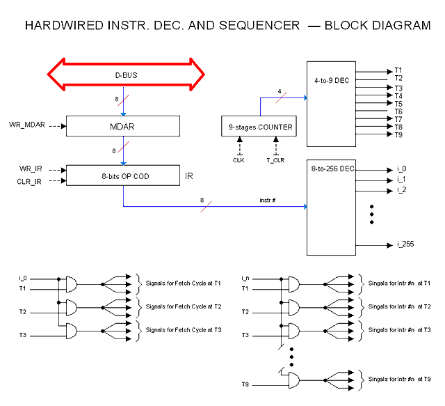
|
The whole purpose of this circuit is to obtain the exact control signals that we need for each clock cycle (T) for each instruction (i). In this view, Op Code Fetch (i_0) is just a particular case.
Note that the instruction byte is not read directly from the bus into the IR register but in the MDAR register instead. This is because we need the OP COD to be available along the entire life of the instruction cycle; we would lose it otherwise when reading an operand from the bus. When reading operands, they are read into MDAR while IR keeps the op cod for the rest of the instruction cycle. Signals WR_MDAR (latch into MDAR from the bus) and WR_IR (latch into IR from MDAR) are not simultaneous but separated in time by half a clock period.
We obtain signals T1 ... T9 (instruction "age") from the main clock, as illustrated. Separately we obtain signals i_0, i_1 ... i_255 (instruction being processed) from the op code.
For each instruction implemented in the CPU there is a simple logic similar to the one shown. It just combines each i_n signal with each Tm signal to provide the control signals needed for instruction, for time. In particular, there is a logic for i_0 (lower left corner in the diagram) which produces the sequence for the Op Code Fetch Cycle.
Signals internal to the IDS such as WR_MDAR, WR_IR, CLR_IR etc. are generated too from these little logic blocks. In particular each instruction must end its sequence by clearing the counter (T_CLR) which forces the appearance of T1, and clearing the IR register (CLR_IR) which forces the next Fetch Cycle.
|
