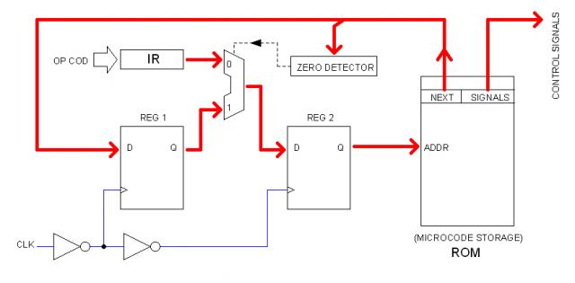
Microcoded FSMThis idea is pretty much borrowed from Bill Buzbee Magic-1 design. It is basically a Finite State Machine (FSM) in which the "next state" (in this case, next microinstruction) is bit-mapped within the microinstruction itself.
As in the Magic-1, the very first block of ROM would contain, one after another, the "first microinstructions" of all instructions so the OP CODE can address them directly. Once the first microinstruction is addressed (from OP CODE), its NEXT field can point to anywhere within the ROM space to continue the instruction sequence.
In address 0 is the HALT instruction which NEXT field is equal to zero. This allows the FSM logic (using the ZERO DETECTOR) to address the ROM from the Instruction Register (IR) rather than from the NEXT field of the current microinstruction.
As per implementation, a detail that I can anticipate is that PROM memories are usually slow (120 ns in contrast with 70ns of typical SRAMs). I have seem 70ns PROMs but they are very expensive. One solution would be to use SRAM instead, being the content dumped from PROM at Power-On time. This is relatively complex due the fact that there is no CPU at Power-On time!
I've been considering a 12 MHz clock because that makes 83 ns cycle, pretty much the typical access time for SRAM chips.
|
Homebuilt CPUs WebRing
JavaScript by Qirien Dhaela
Join the ring?
David Brooks, the designer of the Simplex-III homebrew computer, has founded the Homebuilt CPUs Web Ring. To join, drop David a line, mentioning your page's URL. He will then add it to the list.
You will need to copy this code fragment into your page.
Project start date: May 13 of 2009
|