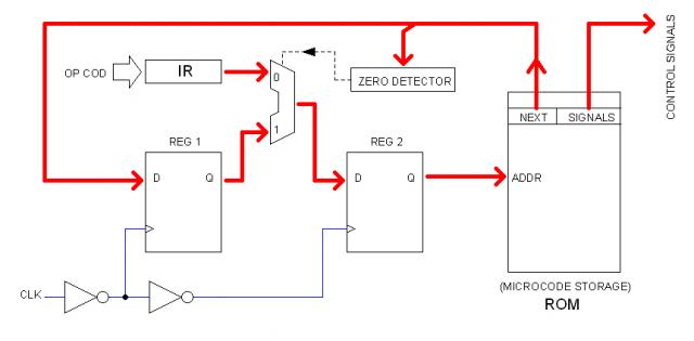
Microcode? Are you sure?Microcoded FSM
This idea is pretty much borrowed from Bill Buzbee Magic-1 design. It is basically a Finite State Machine (FSM) in which the "next state" (in this case, next microinstruction) is bit-mapped within the microinstruction itself.
As in the Magic-1, the very first block of ROM would contain, one after another, the "first microinstructions" of all instructions so the OP CODE can address them directly. Once the first microinstruction is addressed (from OP CODE), its NEXT field can point to anywhere within the ROM space to continue the instruction sequence.
In address 0 is the HALT instruction which NEXT field is equal to zero. This allows the FSM logic (using the ZERO DETECTOR) to address the ROM from the Instruction Register (IR) rather than from the NEXT field of the current microinstruction.
As per implementation, a detail that I can anticipate is that PROM memories are usually slow (120 ns in contrast with 70ns of typical SRAMs). I have seem 70ns PROMs but they are very expensive. One solution would be to use SRAM instead, being the content dumped from PROM at Power-On time. This is relatively complex due the fact that there is no CPU at Power-On time!
I've been considering a 12 MHz clock because that makes 83 ns cycle, pretty much the typical access time for SRAM chips.
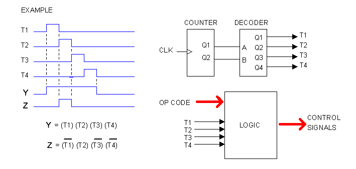
Hard-Wired Intruction Decoder and Sequencer
Microcode is not the only way to go. We can also decode instructions by pure (hard-wired) logic, as illustrated below.
Let's imagine that the CPU will take 4 clocks to fetch and execute the longest instruction. Let's imagine also that most instructions contain bit-mapped fields so many control signal derive directly from the instruction itself. In the diagram above, OP CODE refers to just that: the Operational Code (without the bit-mapped fields).
Here, T1, T2, T3 and T4 are actual signals. They are easy to obtain from a counter and a 2-to-4 bits decoder, as illustrated.
The time-diagram on the left is an hypothetical example showing two control signals: Y and Z. Both signals can be represented as products of T1, T2, T3 and T4. This would be for one instruction only; for different instructions, Y and Z will take different products, depending upon the OP CODE, so the equation for each control signal takes this generic form:
Y = (T1) (T2) (T3) (T4) (OP_CODE)
In other words, any control signal can be produced by the mean of a combinational logic which inputs are: T1, T2, T3, T4 and the OP CODE, as illustrated in the diagram.
In practice, OP CODE will not be too wide since the instructions will devote most of their bits to encoded fields, as mentioned before. Control signals, however, will be quite numerous, in the order of 50 maybe. But I suspect that the Logic circuit can be dramatically simplified using those simplification technics we all learned at school.
As per implementation, I suspect that this can be built very easily using a PLD chips (such as ATMEL ATF2210C) rather than discrete SSI/MSI logic.
|
Homebuilt CPUs WebRing
JavaScript by Qirien Dhaela
Join the ring?
David Brooks, the designer of the Simplex-III homebrew computer, has founded the Homebuilt CPUs Web Ring. To join, drop David a line, mentioning your page's URL. He will then add it to the list.
You will need to copy this code fragment into your page.
Project start date: May 13 of 2009
|