NotesSpeed and components
The slowest component will set the speed of the computer, hence the need for picking the right kind.
CMOS 40xx series, for examples, are too slow, with propagation delays in the order of 100 ns. This is slower that most static RAM chips. HCMOS chips, in contrast, are very fast with propagation delays some times less than 10 ns (6 ns for 74HC00).
For registers, 74C374 gives me 165 ns from clock to latch. In contrast, 74HC374 gives me 20 ns. Same access time (20 ns) is found in SRAM 32Kx8 chip CY7C199CN from Cypress; I would use that chip for building the "Matrix" which is part of the CPU. 74LS series is even faster, but it is also more expensive; for my purposes, HC is OK.
As per PLDs, they are very fast. Amtel ATF22V10C for example (a good candidate for the Heritage/1) doesn't have any figure greater than 10 ns. Time from clock to output, for example, is 2 ns.
It seems then that the interval between control signals can be set around 20 ns. This makes a clock speed of 50 MHz, which is an impressive figure (I was thinking of 12 MHz before) but it's too early for making decisions about clock speed because no circuit have been designed yet. I just wanted to run some numbers and see where they would take me.
What is clear is that CMOS 40xx series are not use, so I shall employ HCMOS components instead.
Machine Cycles
Point, Open, Take
Any data transfer within the computer occurs always between two storage devices. By "storage" we mean any kind of device capable of holding data, such as a CPU register, a memory cell or an UART buffer.
Usually, the transfer takes three steps in time. First, both devices needs to be addressed. Second, the source devices needs to be opened to the bus. Third, the destination device needs to be clocked to latch the data from the bus. We call these steps: Point, Open and Take respectively. Each step has a duraction calculated to allow data to estabilize before commiting the operation.
The sequence of these steps is called a Machine Cycle (MC). There are different types of MCs as we shall see, but they are all essencially the same: Point (address), Open (three-state buffer) and Take (clock latch device). Some times we can skip one or two steps, making the MC shorter.
Fetch and Execute Cycles
In the following time diagram, T1, T2 and T3 constitute the steps mentioned before: Point, Open, Take respectively. Green traces represent sigals in bus lines whereas blue ones represent internal control signals (name indicated between brackets).
The naming convention for internal control signals is this:
OP_DEV
Where OP (operation) can be either RD (read, that is open the three-state buffer to the bus) or WR (write, that is clock the device to latch the input from the bus). And DEV (device) can be a register or any other storage device.
The diagram shows a complete instruction cycle for an indirect address operation. The memory location pointed by 20-bits register Y will be written from register A.
This instruction completes in two machine cycles: Fetch and Execute. The thing to notice is how different control signals appear in time to perform "Point", "Open", "Take" operations over different devices. The duration of T pulses should be big enough to allow data to stabilize before commitment.
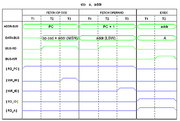
Fetch Operand Cycle
A memory-read cycle for 16-bits data reads a word from memory. An instruction such as
movi a, value ; a <- value (16-bits)
can complete in three machine cycles: Fetch OP-Code, Fetch Operand, Execute. For 20-bits operands, the mechanism is different. A 20-bits operand is needed for direct address instructions such as this:
sto a, addr ; [addr] <- a (addr is 20-bits)
It is also needed for Immmediate 20-bits instructions such as this:
movi sp, value ; sp <- value (20-bits)
In both cases, the least significant 16 bits word (LSW) of the 20-bits address or value is given in the word following the instruction. The most significant 4-bits nibble (MSN) is embedded within the OP-CODE. Thus such instructions can complete in three machine cycles as the following figure shows.
Control signals RD_ID and WR_ID applies to a special 20-bits register that I called "ID" in the drawing but I will call it "MDR" instead. Its sole mission is to hold the operand so it is available to the Exectute cycle. Yes, in the Heritage/1 the MDR register is the size of the Address Bus and there is no MAR register.
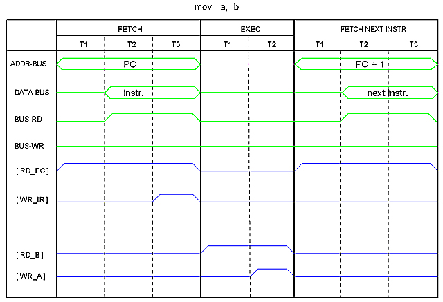
Register-to-Register
Transfer between registers don't require the "Point" step because registers are implicitly addressed by the OP CODE. In the time diagram below, EXEC machine cycle, T1 is an "Open" step and T2 is a "Take" step.
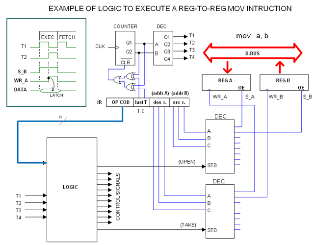
The following figure illustrates how this could be made in practice. Please know that this is not a definite design but only an illustration to the idea.
The instruction code shown in the figure presents two 3-bits fields to encode the destination and source register respectively. This bits are wired to respective decoders which in turn provide all S_reg. (select, that is, open) and WR_reg. (write, that is clock to latch) for all registers. In the example we have assumed eight registers in the CPU.
Note that one of these decoders (the one in the top) is dedicated to S_reg. signals whereas the other is dedicated to WR_reg. signals. The encoders also have an "strobe" input, so they will output nothing until the strobe signal is present and this comes from the Instruction Decoder Logic.
This logic takes the OP COD as input and it also takes the synchronization signals T1, T2, T3, T4. Those signals are obtaining from a 2-to-4 decoder fed from a 2-bits counter which in turn is clocked from the master clock.
We have seen that most instructions takes three steps (T1, T2, T3), but this takes only two. The solution is to provide a "shortcut" by reseting the counter so the decoder can jump to T1.
For that purpose, the Instruction have a 2-bits field termed "last T". The content is constantly compared with the counter output as we can see in the diagram. In this case, last T is equal 2, so as soon as T3 tries to appear, it will be forced to become T1.
The Logic is designed so signals S_B and WR_A appear as shown in the timing diagram. Then the counter is reset, as it is IR, so the next cycle will be, with no choice, a fetch cycle.
Register Increment / Decrement
Registers suitable for increment/decrement operations are implemented with binary counter chips. This means that increment/decrement instructions (such as INCR Y) do not involve data transfer and can be therefore performed in one single step, that is during T1.
Synchronizing with slow Peripherals
Peripherals for the Heritage/1 must be designed so they communicate with the Bus via three-state high-speed buffers such as the 74HC374. This is because the CPU will read and write the device (that is the buffer) at the same speed it does for static RAM memory. This means that, when reading from a peripheral, any delay introduced by the device itself must lie between the moment it is addressed and that in which the buffer got a valid data read from the device.
During this period (from addressing to data ready) the device must activate and keep active a bus line termed WAIT. The device will deactivate that line once the data has been safely transferred to the buffer.
The CPU samples the WAIT line during both "Open" and "Take" steps of every Memory Read cycle, that is T2 and T3 (remember that peripherals are memory mapped). If WAIT is active, the RD and WR signals are not activated, the IR register is not cleared and PC not incremented. This results into the same Machine Cycle being repeated over and over until the WAIT signal is removed by the device so the data (from the buffer) can be read as normal.
If an interrupt occurs while the CPU is waiting, it will be served. Upon return a new Machine Cycle will automatically resume the waiting condition.
Similar mechanism apply to write operations. The CPU will sample the WAIT line before rasing the WR signal in T2. Most likely the first time it will success since the data is written to a high speed buffer in the Peripheral circuitry. As soon as it is received, the peripheral will activate the WAIT line and will keep it active until it is ready for the next one. This implies that, when writting bulk data to a peripheral, the CPU will success the first but it will have to insert wait machine cycles for all others.
Proper design of peripherals will include, of course, the use of multibyte FIFO buffers. Those need to be 16 bits wide (the size of the Heritage/1 Data Bus); remember that this computer cannot address bytes individually.
The WAIT signal is then used to indicate buffer full condition.
Addressing Modes
The Heritage/1 features 16-bits general purpose registers and 20-bits address oriented registers. Such disparity makes transfers between registers of different sizes kind of odd. In order to fix this insanity I've came with RISC-like techniques leading to special immediate addressing modes for 20 bits registers.
Immediate 16 bits
This is the normal immediate addressing mode, common to most computers. It takes two consecutive words in memory: the op. cod. and the 16-bits operand.
Example:
movi a, value
Immediate 20 bits
To load a 20-bis register from memory would take two operands, but this would waste 12 bits from the second operand. The (RISC like) solution is to embed the most significant nibble (MSN) within the op. code. Therefore, an instruction of this kind takes only one operand from memory and can complete in two machine cycles.
Example:
movi sp, value ; Value is 20 bits but it only takes one 16-bits operand.
; the remaining 4 bits (MSN) is embedded in the op code.
Immediate 20 bits nibble high
When transferring data from a 16-bits register to a 20-bits register, only the 16 least significant bits are copied. The upper nibble can then be supplied by the mean of an "Immediate 20 bits nibble high" instruction which will write the 4 most significant bits leaving the rest untouched.
Example:
mov sp, a ; sp <- least significant 16 bits
movih sp, value ; sp <- most signifant 4 bits (value is 4 bits).
Immediate 20 bits nibble high intructions only takes one step (T1) of the Execute Machine Cycle since the operand is embedded within the op code. No bus operation is performed during this cycle.
The ALU/Accumulator partnership
In the Heritage/1 (as in most computers) the Accumulator register (A) holds the result of the last ALU operation. Additionally, it serve as a general purpose register. The ALU has two 16 bits inputs: A and whatever is in the Data Bus.
The figure below illustrates the relationship between A, the ALU and the Data Bus.
Control signal S_ALU (Select ALU) causes the ALU output to be routed to the Accumulator's input. When S_ALU is not active, the Accumulator is fed from the Data Bus instead so it can be used as general purpose register.
Signal S_A opens the Accumulator's output to the bus. We activate this signal when we want to read from A.
Signal WR_A clocks the Accumulator so whatever is at the input, gets latched. We activate this signal to write A from the Data Bus (example: mov a, b); the signal will actually commit the transfer. For performing logical or arithmetic operations, the same signal will commit the operation but in this case, S_ALU must be active.
Finally, the signal f (which takes n bits) defines the ALU operation to be performed.
We can see the ALU and the Accumulator as being part of the same circuit. The following figure illustrate such vision.
The signal S_ALU decides whether the box will behave as ALU or general purpose register A. In the lastest, signal S_A will be used to read from A whereas signal WR_A will be used to write (latch) toward A.
Register B is similar in the sense that the signal WR_B actually clocks its latches whereas S_B opens its three-state buffers to the BUS so others can read it. It is not shown in the figure but one can imagine.
Finally, here is a timing diagram of two operations with the A/ALU unit. We assume that f (not shown in the diagram) contains the code for the SUM operation.
During the first clock cycle, A is latched with the sum of itself and whatever is in the bus (B in this case). In a further clock cycle, B is moved to A.
The A/ALU unit will be most likely implemented with PLD whereas other registers will be built with 74HC374 chips.
|