OperationThe Heritage/1 is operated similar to 1960's and 1970's minicomputers. When powered-on, the computer has no software in it so it does basically nothing.
Once the computer is powered-on, the operator uses the Console to load the desired software from storage. Before doing that, however, a little "loader" program needs to be entered manually using the Console's Entry switches.
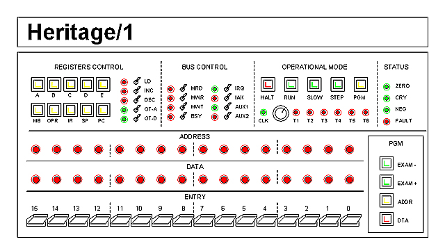
The Console
The Heritage/1 Console is very simple. It consists of two parts: The bottom half is designed for "programming", that is entering code into main memory. The upper half is designed to facilitate low level software and circuitry debugging.
The computer can operates in four different Operational Modes: RUN, SLOW, STEP and PROGRAMMING. It can also be Halt. The desired Operational Mode can be set from the OPERATIONAL MODE block. After power-on or reset, the computer is in Halt condition.
While in RUN mode, the computer operates at full speed. In SLOW mode, the system clock is replaced with a very slow one (several Hertz) which frequency can be adjusted using the rotary knob. When in STEP mode, the computers halts after the current instruction has finished execution; pressing the STEP button again causes the next instruction to be fetched and executed. When putted in PGM mode, the programmer block at the bottom can be used.
Bus content and different control signals are constantly monitored by LEDs no matter the current Operational Mode. The DATA and ADDRESS LEDs monitor the internal Address and Data buses respectively. Specially useful is the FAULT LED which lights to indicate a CPU exception condition. After a fault, the computer halts automatically.
Working in Programming Mode (PGM)
To enter Programming Mode, the operator presses the PGM button in the OPERATIONAL MODE block. Buttons in the PGM block illuminate to indicate that they can now be used (they are ignored in RUN and SLOW modes). The ADDRESS and DATA LEDs now show the address and content respectively from the default memory location; this has been set using an internal DIP switch.
Buttons EXAM- and EXAM+ can be used to navigate the memory from that point back and forward respectively. For each time, a memory read cycle is performed for updating the LEDs reading. If a different address is needed, this can be entered using the ENTRY switches, then pressing the ADDR button. The ADDRESS and DATA LEDs will then show the new address and content respectively.
To modify memory content, the operator enters the desired value using the ENTRY switches, then he presses the DTA button; this causes the new content to be written to memory and the address to be automatically incremented. This implies that, upon DTA button pressed, the address and data shown in the LEDs correspond, not to that just modified but to the one immediately next.
If, for instance, the operator wants to fill a block of memory with a given fixed data value, he needs to proceed as following:
1.- Enter the desired base address in the ENTRY switches.
2.- Press the ADDR button. Both address and memory content will be displayed.
3.- Enter the desired data in the ENTRY switches.
4.- Press the DTA button. Address and content for the next memory location will be displayed.
5.- Press the DTA button repeatedly as many times as needed. For each time, the current location will be written from the switches and the address will be incremented automatically.
A more practical example is to enter a "loader" program that allows the computer to load an existing application from storage.
Once the memory has been modified as desired, the operator enters the initial program address in the ENTRY swithes, presses the ADDR button and then presses the RUN button to star running the program. It can also chose to run the program in SLOW or STEP modes.
The computer can be halt at any time by pressing the HALT button in the OPERATIONAL MODE block.
Low-level Debugging (HALT)
When the computer is in Halt condition, switches in the REGISTERS CONTROL and BUS CONTROL blocks can be used. They are ignored otherwise.
The REGISTERS CONTROL block allows the engineer to load, increment, decrement, open to the internal data bus (D-BUS) or to the internal address bus (A-BUS) any of the CPU registers. The BUS CONTROL block allows to manually manage the external U-BUS control signals. Eventually the computer can be ran completely manual from those blocks. Even a system clock can be asserted by pressing the Halt button.
We can also write content to internal A-BUS and D-BUS from the ENTRY switchers. Now, the EXAM- and EXAM+ in the PGM block are not operational so they are not illuminated. ADDR and DTA buttons, however, are illuminated to indicate that we can used them, only that in different manner respect to that in Programming Mode.
Whatever is in the ENTRY switches can be passed to the internal D-BUS by pressing the DTA button in the PGM block. The switches content will simply be opened to the D-BUS, not written to memory. The value will not be latched either, so we will need to press and hold the DTA button as long as we need it to be present in the bus. The previous also applies to the A-BUS and the ADDR button.
Running a program (RUN, SLOW, STEP)
Running a program is different depending on the previous Operational Mode.
If the RUN (or SLOW or STEP) button is pressed while the computer is in PROGRAMMING mode, then the initial address is the one entered in the ENTRY switches. To run a program this way the operator needs to enter the initial address with the switches, press the ADDR button, then to press the RUN (or SLOW or STEP) button to initiate execution.
If the RUN (or SLOW or STEP) button is pressed while the computer is in HALT condition, then the initial address is that contained in the Program Counter register (PC). To run a program this way, the engineer loads the initial address into PC, then presses the RUN (or SLOW or STEP) button to initiate execution.
|