The 16-bits Heritage/1I finally decided to forget about that "OS ready" minicomputer and make PREHER/816 (renamed back Heritage/1) the main subject of my project. I also decided to make my machine 16-bits so it is suitable for some useful work in the future.
Tech Info
This book will describe the computer in great detail. For now, it contains the most recent versions of circuits and ideas.
Conditional Status and Flags Register
The Conditional Status describes the result of a data operation. This can be (not exclusive):
Zero (Z): if the result is zero
Negative (N): if the result is negative
Carry (C): Arithmetic carry
Overflow (V): if the result does not fit into the destination
 The S-BUS The S-BUS
Since the Conditional Status refers to a result and this is always kept in some register, detecting status is a job for the register's circuitry. Therefore, each register offers its own means for detecting its own Conditional Status.
The way for registers to deliver their individual status to the Flags register, is by the mean of a 4-bits bus (wired in the Data Slots) called S-BUS.
All registers are constantly generating status signals internally but, at a given time, only one is open to the S-BUS. This is because Flags should only be set according to the register being accessed by the current instruction and only if that instruction is meant to affect flags.
An exception to this rule are those instructions that increment or decrement two registers at the same time (INCM, DECM and INDEC). In this case both registers open to the S-BUS and flags are set as an "OR" of the individual conditions.
There are none dedicated control signals for opening registers to the S-BUS. The selection is made automatically when the register in question is Loaded, Incremented or Decremented.
Registers that do not report status
Registers that are not meant to hold results, won't report conditional status (they are not wired to do so). Those are the following:
-- Program Counter (PC)
-- Stack Pointer (SP)
-- Operand Register (OR)
-- Instruction Register (IR)
The Flags Register (F)
The Flags register (F) resides in the Master Controller card (MC) which plugs to both Data and Control slots. The register is 8-bits but only 4 are used to remember the Conditional Status; a 5th. bit is used to remember the Interrupt Enabled condition as we shall see; the remaining 3 bits are implemented but not used (reserved for future use). The whole register F is saved to the Stack during CALL or Interrupt and restored back upon Return.
The register is actually made out of D-type flip-flops (74ACT74) fed from the S-BUS. The outputs go to another bus (called CS-BUS) wired in the Control Slots; this bus is always open so the current status is always available to Controller cards. Flags are latched selectively using signals LD_FZ, LD_FN, LD_FC and/or LD_FV produced by IDS cards during the last cycle of those instructions that affect flags.
Instructions and Flags
Although further analysis on this topic is still pending , I can anticipate the following:
-- ALU instructions affect all flags (Z,N,C,V).
-- Data transfer instructions (MOV, LD, STO, PUSH, POP) affect flags Z, N.
-- Increment/Decrement instructions affect flags Z, N, V.
-- Branch instructions affect none flag.
By not affecting flags, I mean that the previous status remains. The programmer needs to take this into account when placing conditional branch instructions within the code.
The Interrupt Enabled condition
The necessity of recording the Interrupt Enabled condition as a flag has to do with nested interrupts. When an interrupt service routine (lets call it: ISR1) gets interrupted by a highest priority interrupt (ISR2), the Interrupt Controller disables interrupts before passing control to ISR2. If this routine failed to enable interrupts back, then interrupts would remain disabled when control returns to ISR1, which is not the intended behavior. But, by remembering the Interrupt Enable condition in the Flags register, interrupts will be automatically restored upon return since F had been saved to the Stack.
Thus there is a flip-flop in F for the Interrupt Enable condition, only that its input (SI) and output (CSI) are not wired with the S-BUS and CS-BUS respectively but treated as point-to-point connections. This is because only a few circuits will make use of them; those circuits are: the Interrupt Controller, the IDS card responsible for the DI and EI instructions and the Control Panel.
CPU BACKPLANE
The CPU backplane is constructed on a prototyping board holding six 96-pins DIN41612 female connectors and other six 120-pins DIN41612 female connectors. This divides the backplane into two sections: Data Slots and Control Slots respectively. The former is used for "data oriented cards" (such as registers) and the latest is used for "controller cards".
Each of the two Slot types are wired separate. Most of the wires conforms different buses whereas others serve for point-to-point inter-card connections.
A special card named "Master Controller" features two connectors (one 96-pins and the other 120-pis) and plugs to both Slot types. This card contains those circuits that need access to the two worlds such as the Instruction Register (IR), the "Arbitrer" and others. It also provides the interface (buffering) with the external bus (U-BUS).
Following is the pinout for both Slot types:
Data Slots
- - - - - - - - - - - - - -
A B C
- - - - - - - - - - - - - -
1 GND GND GND
2 D0 PP D8
3 D1 PP D9
4 D2 PP D10
5 D3 PP D11
6 D4 PP D12
7 D5 PP D13
8 D6 PP D14
9 D7 PP D15
10 L0 PP L8
11 L1 PP L9
12 L2 PP L10
13 L3 PP L11
14 L4 PP L12
15 L5 PP L13
16 L6 PP L14
17 L7 PP L15
18 RST PP L16
19 FLT PP L17
20 SZ PP L18
21 SN PP L19
22 SC PP L20
23 SV PP CLK
24 A7 PP A15
25 A6 PP A14
26 A5 PP A13
27 A4 PP A12
28 A3 PP A11
29 A2 PP A10
30 A1 PP A9
31 A0 PP A8
32 +5V +5V +5V
- - - - - - - - - - - - - -
Signals Descriptions:
DO-15 Internal Data Bus
A0-15 Internal Address Bus
L0-20 Internal Lamps Bus
SZ Set Conditional Status Zero
SN Set Conditional Status Negative
SC Set Conditional Status Carry
SV Set Conditional Status Overflow
RST System Reset
CLK System Clock
FLT Fault Condition
PP Point-to-Point Control Signals
Control Slots
Except those marked as "PP" (Point to Poin), all signals in Control Slots are wired together in a Bus.
Signals marked as CTL (Control) are not designated yet but they will as the design progresses.
- - - - - - - - - - - - - -
A B C
- - - - - - - - - - - - - -
1 GND GND GND
2 IR0 PP IR8
3 IR1 PP IR9
4 IR2 PP IR10
5 IR3 PP IR11
6 IR4 PP IR12
7 IR5 PP IR13
8 IR6 PP IR14
9 IR7 PP IR15
10 CTL CTL CTL
11 CTL CTL CTL
12 CTL CTL CTL
13 CTL CTL CTL
14 CTL CTL CTL
15 CTL CTL CTL
16 CTL CTL CTL
17 CTL CTL CTL
18 RST CTL CTL
19 FLT CTL CTL
20 CSZ LD_FZ CTL
21 CSN LD_FN CTL
22 CSC LD_FC CTL
23 CSV LD_FV CLK
24 CTL CTL CTL
25 CTL CTL CTL
26 CTL CTL CTL
27 CTL CTL CTL
28 CTL CTL CTL
29 CTL CTL CTL
30 CTL CTL CTL
31 CTL CTL CTL
32 CTL CTL CTL
33 CTL CTL CTL
34 CTL CTL CTL
35 CTL CTL S1
36 CTL CTL S0
37 CTL CTL EOE
38 CTL CTL ET1
39 CTL CTL ET0
40 +5V +5V +5V
- - - - - - - - - - - - - -
Signals Descriptions:
IR0-15 Instruction Register Output
CSZ Conditional Status Zero
CSN Conditional Status Negative
CSC Conditional Status Carry
CSV Conditional Status Overflow
LD_FZ Load Flag Zero
LD_FN Load Flag Negative
LD_FC Load Flag Carry
LD_FV Load Flag Overflow
S0, S1 Operational Status
ET0, ET1 Enconded Time (T1, T2, T3, T4)
RST System Reset
CLK System Clock
FLT Fault Condition
CTL Control Signals (Bus)
PP Control signals (Point-to-Point)
Encoded Time:
- - - - - - - - -
ET1 ET0 Time
- - - - - - - - -
0 0 T1
0 1 T2
1 0 T3
1 1 T4
- - - - - - - - -
Operational Status:
- - - - - - - - - - - - - - - - - - - -
S1 S0 Operational Status
- - - - - - - - - - - - - - - - - - - -
0 0 Halt
0 1 Fetch
1 0 Execute
1 1 Interrupt being negotiated
- - - - - - - - - - - - - - - - - - - -
Operation
The Heritage/1 is operated similar to 1960's and 1970's minicomputers. When powered-on, the computer has no software in it so it does basically nothing.
Once the computer is powered-on, the operator uses the Console to load the desired software from storage. Before doing that, however, a little "loader" program needs to be entered manually using the Console's Entry switches.
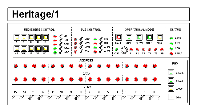
The Console
The Heritage/1 Console is very simple. It consists of two parts: The bottom half is designed for "programming", that is entering code into main memory. The upper half is designed to facilitate low level software and circuitry debugging.
The computer can operates in four different Operational Modes: RUN, SLOW, STEP and PROGRAMMING. It can also be Halt. The desired Operational Mode can be set from the OPERATIONAL MODE block. After power-on or reset, the computer is in Halt condition.
While in RUN mode, the computer operates at full speed. In SLOW mode, the system clock is replaced with a very slow one (several Hertz) which frequency can be adjusted using the rotary knob. When in STEP mode, the computers halts after the current instruction has finished execution; pressing the STEP button again causes the next instruction to be fetched and executed. When putted in PGM mode, the programmer block at the bottom can be used.
Bus content and different control signals are constantly monitored by LEDs no matter the current Operational Mode. The DATA and ADDRESS LEDs monitor the internal Address and Data buses respectively. Specially useful is the FAULT LED which lights to indicate a CPU exception condition. After a fault, the computer halts automatically.
Working in Programming Mode (PGM)
To enter Programming Mode, the operator presses the PGM button in the OPERATIONAL MODE block. Buttons in the PGM block illuminate to indicate that they can now be used (they are ignored in RUN and SLOW modes). The ADDRESS and DATA LEDs now show the address and content respectively from the default memory location; this has been set using an internal DIP switch.
Buttons EXAM- and EXAM+ can be used to navigate the memory from that point back and forward respectively. For each time, a memory read cycle is performed for updating the LEDs reading. If a different address is needed, this can be entered using the ENTRY switches, then pressing the ADDR button. The ADDRESS and DATA LEDs will then show the new address and content respectively.
To modify memory content, the operator enters the desired value using the ENTRY switches, then he presses the DTA button; this causes the new content to be written to memory and the address to be automatically incremented. This implies that, upon DTA button pressed, the address and data shown in the LEDs correspond, not to that just modified but to the one immediately next.
If, for instance, the operator wants to fill a block of memory with a given fixed data value, he needs to proceed as following:
1.- Enter the desired base address in the ENTRY switches.
2.- Press the ADDR button. Both address and memory content will be displayed.
3.- Enter the desired data in the ENTRY switches.
4.- Press the DTA button. Address and content for the next memory location will be displayed.
5.- Press the DTA button repeatedly as many times as needed. For each time, the current location will be written from the switches and the address will be incremented automatically.
A more practical example is to enter a "loader" program that allows the computer to load an existing application from storage.
Once the memory has been modified as desired, the operator enters the initial program address in the ENTRY swithes, presses the ADDR button and then presses the RUN button to star running the program. It can also chose to run the program in SLOW or STEP modes.
The computer can be halt at any time by pressing the HALT button in the OPERATIONAL MODE block.
Low-level Debugging (HALT)
When the computer is in Halt condition, switches in the REGISTERS CONTROL and BUS CONTROL blocks can be used. They are ignored otherwise.
The REGISTERS CONTROL block allows the engineer to load, increment, decrement, open to the internal data bus (D-BUS) or to the internal address bus (A-BUS) any of the CPU registers. The BUS CONTROL block allows to manually manage the external U-BUS control signals. Eventually the computer can be ran completely manual from those blocks. Even a system clock can be asserted by pressing the Halt button.
We can also write content to internal A-BUS and D-BUS from the ENTRY switchers. Now, the EXAM- and EXAM+ in the PGM block are not operational so they are not illuminated. ADDR and DTA buttons, however, are illuminated to indicate that we can used them, only that in different manner respect to that in Programming Mode.
Whatever is in the ENTRY switches can be passed to the internal D-BUS by pressing the DTA button in the PGM block. The switches content will simply be opened to the D-BUS, not written to memory. The value will not be latched either, so we will need to press and hold the DTA button as long as we need it to be present in the bus. The previous also applies to the A-BUS and the ADDR button.
Running a program (RUN, SLOW, STEP)
Running a program is different depending on the previous Operational Mode.
If the RUN (or SLOW or STEP) button is pressed while the computer is in PROGRAMMING mode, then the initial address is the one entered in the ENTRY switches. To run a program this way the operator needs to enter the initial address with the switches, press the ADDR button, then to press the RUN (or SLOW or STEP) button to initiate execution.
If the RUN (or SLOW or STEP) button is pressed while the computer is in HALT condition, then the initial address is that contained in the Program Counter register (PC). To run a program this way, the engineer loads the initial address into PC, then presses the RUN (or SLOW or STEP) button to initiate execution.
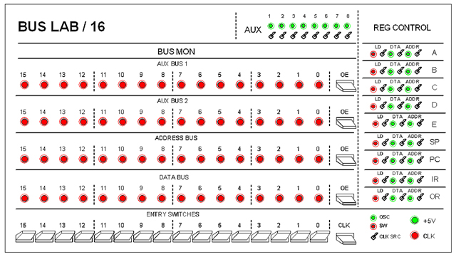
BUS LAB
Before going further, I will build this development tool that I called BUS LAB. It is basically a manual-signals generator and monitoring tool that will provide control signals (Switches) and will monitor buses status (LEDs) to be used in circuits under testing.
Operation
Though designed with the Heritage/1 in mind, this BUS-LAB is a generic tool (I think).
Once connected to the LAB, buses in the target circuit are constantly monitored by LEDs in the BUS MON block of the LAB's front panel. Additional (8) signals can be monitored in the AUX block.
ENTRY SWITCHES write data to the selected bus. Switches labeled "OE" in each bus open a 3-State buffer from the switches to that bus. Caution must be observed for not to open more than one of the OE switches as the same time.
The switches and LEDs in the REG CONTROL block provide manual control signals to the different registers. Switches in the AUX block can be used for same purpose.
Finally is the CLOCK section at the bottom. The "CLK SRC" switch selects the source for the clock; this can be either an oscillator provided by the LAB or the CLK switch. The resulting clock signal is monitored by the CLK LED.
Power (regulated 5V) is provided too. This is monitored by the "+5V" LED.
Buses and the CPU Backplane
Heritage/1 units are interconnected via an external bus called U-BUS; each unit in turn possesses its own specific internal bus. Within a unit, all inter-card connections are made via a Backplane made of 96-pins DIN 41612 connectors. Two different kinds of connections exists: buses and point-to-point; this implies that frame slots are not generic but dedicated, that is cards cannot be placed anywhere within the frame but in their designated slots.
CPU internal busses are: D-BUS (data), A-BUS (address), S-BUS (conditional status flags), C-BUS (internal control signals) and T-BUS (instruction sequence count). A Bus Controller Card not plugged to the Backplane but placed behind it, provides the necessary interface to the external U-BUS.
External Bus (U-BUS)
The U-BUS consists of two ribbon cables termed A and B respectively, ended with D-SUB connectors that plug from unit to unit in Daisy-Chain topology. Signals in the U-BUS are the following (NOTE: The actual pin-out has not been defined yet):
CABLE A (D-SUB 25)
- - - - - - - - - -
ADDR LOWER : A0-15
ADDR UPPER : A16-23
CABLE B (D-SUB 37)
- - - - - - - - - -
DATA : D0-15
CONTROL : MRD, MWR, MWT, IRQ, IAK, BSY, SRT
RESERVED : Future use (13)
Power (+5V) is not present in the U-BUS since units are self-powered.
Control Signals in the U-BUS
MDR: Memory Read
MWR: Memory Write
MWT: Wait (for synchronization with slow devices)
IRQ: Interrupt Request
IAK: Interrupt Acknowledge
BSY: Bus busy (not in 3rd. state)
SRT: System Reset
Note: Peripherals are memory mapped.
CPU Internal Bus (Backplane)
CPU Backplane slots are classified into two classes: DATA SLOTS (for data oriented cards such as the ALU and registers cards) and CONTROL SLOTS (for controller cards such as IDS and Interrupt Controller).
The pin-out adopted is identical to the industrial standard VME Bus P1, except for those signals not used in the Heritage/1. Point-to-point signals and Heritage/1 specific buses have been added in place of those.
Data Slots
The table below shows the resulting pin out for DATA SLOTS. Signals labeled CTL are for point-to-point connections mostly internal control signals. Some other signals have been added such as: SR (System Reset) and CSZ, CSN, CSC (Conditional Status Zero, Negative and Carry, respectively).
A B C
- - - - - - - - - - - -
1 DO CTL D8
2 D1 SR D9
3 D2 CTL D10
4 D3 CTL D11
5 D4 CSZ D12
6 D5 CSN D13
7 D6 CSC D14
8 D7 CS3 D15
9 GND CS4 GND
10 CLK CS5 CTL
11 GND CS6 CTL
12 CTL CS7 CTL
13 CTL CTL CTL
14 CTL CTL CTL
15 GND CTL CTL
16 CTL CTL CTL
17 GND CTL CTL
18 CTL CTL CTL
19 GND CTL CTL
20 CTL GND CTL
21 CTL CTL CTL
22 CTL CTL CTL
23 CTL GND A15
24 A7 CTL A14
25 A6 CTL A13
26 A5 CTL A12
27 A4 CTL A11
28 A3 CTL A10
29 A2 CTL A9
30 A1 A0 A8
31 CTL CTL CTL
32 +5V +5V +5V
Control Slots
For Control Slots, same control pins plus the 16 address lines (not used by IDS cards) are wired in three local control buses: C-BUS, S-BUS and T-BUS. Lines D0-15 are not wired from the internal Data Bus as in Data Slots but directly from the Instruction Register (IR).
The table below shows the pin out for Control Slots.
A B C
- - - - - - - - - - - -
1 DO SF D8
2 D1 SR D9
3 D2 S0 D10
4 D3 S1 D11
5 D4 CSZ D12
6 D5 CSN D13
7 D6 CSC D14
8 D7 CS3 D15
9 GND CS4 GND
10 CLK CS5 IE
11 GND CS6 CTL
12 ET0 CS7 CTL
13 ET1 CCS CTL
14 ET2 CTL CTL
15 GND CTL CTL
16 CTL CTL CTL
17 GND CTL CTL
18 CTL CTL CTL
19 GND CTL CTL
20 CTL GND CTL
21 CTL CTL CTL
22 CTL CTL CTL
23 CTL GND CTL
24 CTL CTL CTL
25 CTL CTL CTL
26 CTL CTL CTL
27 CTL CTL CTL
28 CTL CTL CTL
29 CTL CTL CTL
30 CTL CTL CTL
31 CTL CTL CTL
32 +5V +5V +5V
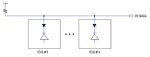
Control Bus (C-BUS)
The purpose of wiring all control signals in a bus is to allow different controllers (such as IDSs and the Interrupt Controller) to manage the same control lines as illustrated in the figure below:
Status Bus (S-BUS)
SF Fetch Cycle
SR System Reset
S0 Operational Status
S1 Operational Status
CSZ Conditional Status Zero
CSN Conditional Status Negative
CSC Conditional Status Carry
CS3 Conditional Status (Reserved)
CS4 Conditional Status (Reserved)
CS5 Conditional Status (Reserved)
CS6 Conditional Status (Reserved)
CS7 Conditional Status (Reserved)
CCS Clear Conditonal Status
IE Interrupt Enabled
SF signal is activated by instruction decoding logic (located at IDS cards) during the falling edge
of the last clock cycle of every instruction. The signal is used to syncrhonically clear both IR and the T-Counter; this action forces an Op Code Fetch Cycle taking place with the next clock rising edge.
S0, S1 define the current Operational Status according to the following table:
- - - - - - - - - - - - - - - - - - - - - - - - - - - - - - -
S1 S0 Operational Status
- - - - - - - - - - - - - - - - - - - - - - - - - - - - - - -
0 0 Halt
0 1 Interrupt being negotiated (before ISR is called)
1 0 IDS having control in Step mode
1 1 IDS having control in Run mode
- - - - - - - - - - - - - - - - - - - - - - - - - - - - - - -
If S1=0, IDS card ihibit themselves so other circuit (such as the Interrupt Controller or the Console) can take control of the machine. When S1=S0=1 and interrupt is enabled (IE=0), the Interrupt Controller card is allowed to serve interrupts. In that event, the Interrupt Controller will pull signal S1 down to zero for inhibiting IDS cards so it can take control of the machine while negotiating the interrupt with the interrupter device (see Interrupt life-time).
Conditional Status signals come from the Flags Registers (F). The first three are defined: CSZ, CSN, CSC; the other five (CS3-7) are reserved for future use. These signals are set from data oriented circuits; for instance, a register been cleared by an instruction will activate the CSZ signal). The signal CCS (activated by a controller such as an IDS card) will clear all flags at once.
Sequence Bus (T-BUS)
The T-BUS is fed from the "Sequece Counter" and represent the encoded clock cycles: T1, T2, ... T6. Actual signals are termed "ETi" for "encoded time":
ET0
ET1
ET2
Note: ET0 = ET1 = ET2 = 0 represents T1.
Bus Controller Card
The Bus Controller is not plugged to the Backplane as a normal card but instead placed behind it and connected using a different set of connectors. It serves to different purposes.
Bus Interface
The Bus Controller Card buffers the external bus (U-BUS) providing a bridge to the internal buses.
Arbitrator
The Computer Console is capable of taking over controller cards for different operational modes. The Bus Controller arbitrates between the two, passing control to one or another depending of the current mode. For this to be possible, all internal control signals, as well as the S-BUS, connects directly to the Bus Controller card. The Console Controller connects directly to this card too.
Instruction and Memory Bank registers
The Bus Controller contains the Instruction Register (IR). This is in order to provide the IR output to lines D0-15 in IDS Slots while taking the IR input from the D-BUS wired in Data Slots.
It also contains the Memory Bank register (MB). This is because the input for this register comes directly from the IR and the output only goes to the external U-BUS (A16-23).
|