General Theory of OperationInternally, the CPU works very similar to a clock's machinery. Nearly all internal activities consists of sequences of internal control signals. Some sequences are built automatically, others are built as instructed in the current instruction's operational code.
Control Signals
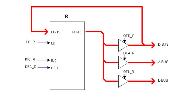
The figure below represents a typical Heritage/1 register as an example of a circuit being controled by internal control signals.
The circuit encapsulated into the box can latch a 16-bits word. It can also increment or decrement its content. Latched content is always available at the Q0-15 outputs but those are isolated from the buses by the mean of three 3-state buffers as shown.
Control signal LD_R makes the register to latch its inputs D0-15 which are connected directly to the D-BUS. Signals INC_R and DEC_R makes the content to increment or decrement respectively.
In order to expose the register's content to the D-BUS, signal OTD_R must be present. Similarly signal OTA_R makes the content available to the A-BUS and OTL_L, to the L-BUS. This later is the "lamps bus" which content is always shown in the Console's Data Lamps (LEDs).
The naming convention for control signals is: SIGNAL_RESOURCE as in LD_R (Load register R). Common prefixes are (among others):
LD_ Load (clock to latch)
OTD_ Output To Data (open buffer to D-BUS)
OTA_ Output To Address (open buffer to A-BUS)
OTL_ Output To Lamps (open buffer to L-BUS, the "lamps" bus)
INC_ Increment
DEC_ Decrement
All control signals are active low with no exception. This makes it easier to "OR-them" using diodes.
Sequences
The previous example makes it clear the need for sequences. For example, to move content from register B to register A, the following sequence is needed:
1.- Open register B to the D-BUS by activating the OTD_B signal.
2.- Load register A from the D-BUS by activating LD_A, while keep OTD_B active.
3.- Deactivate both OTD_B and LD_A.
Sequences are synchronous with the computer master clock (CLK). A central counter named T-COUNTER (clocked by the master clock) generates two "encoded-time" signals named ET0 and ET1 respectively. Sequences are actually built by combinatorial logic using ET0, ET1 as inputs.
The four possible combinations for ET0, ET1 are conventionally named: T1, T2, T3, T4 as following:
ET1 ET0 T
----------------
0 0 T1
0 1 T2
1 0 T3
1 1 T4
----------------
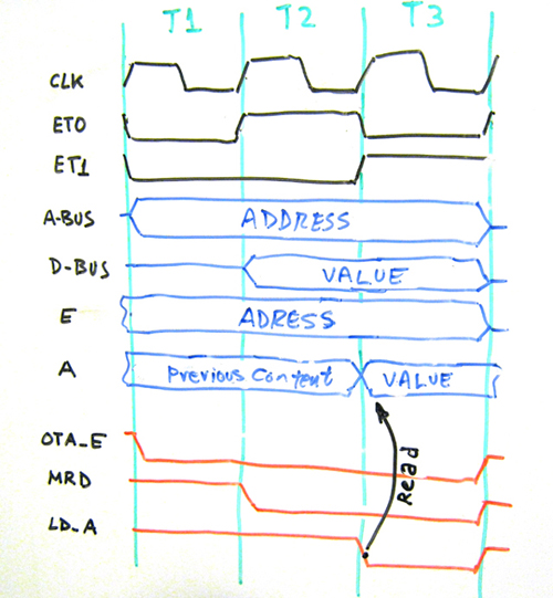
The time diagram below illustrates the execute cycle for the instruction:
ldx a, e
This instruction reads the memory location pointed by register E, into register A.
The time diagram shows the sequence of control signals OTA_E, MRD, LD_A needed to execute the given instruction. MRD (Memory Read) is an external signal present in the U-BUS wired to open the memory chip buffers to the Data Bus.
As shown, signals activate and deactivate at CLK period intervals as result of changes in ET0, ET1. The master clock (CLK) is currently 4 MHz thus this particular sequence takes 750 ns to complete. The shortest sequence in Heritage/1 takes one clock period (250 ns); the longest takes eight (2 us).
As mentioned, all sequences are built from ET0, ET1. The only exceptions are of those built by the Console; this exception has been made in order to minimize dependencies since the Console is meant to be the ultimate resource to control de computer in case of failure.
Building sequences with combinatorial logic
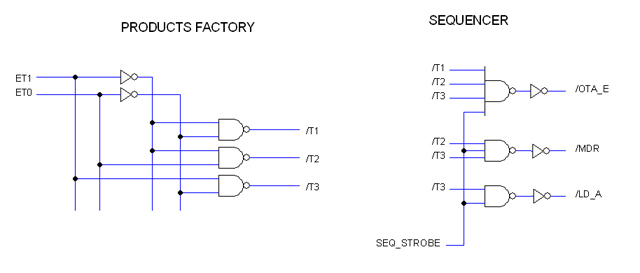
As an example, we will design a circuit to generate the sequence of previous section. The circuit will take signals ET0, ET1 as inputs to generate /OTA_E, /MRD, /LD_A as outputs.
Note: We use a forward slash (/) to denote logic inversion.
From the time-diagram on previous section we can directly deduct the equations. In order to make things simpler we will mentally invert the control signals OTA_E, MRD, LD_A so they will become active-high as opposite as shown in the diagram. The resulting equations are these:
OTA_E = T1 + T2 + T3
MRD = T2 + T3
LD_A = T3
Where T1, T2 and T3 are products of E0, E1 as following:
T1 = /ET1 * /ET0
T2 = /ET1 * ET0
T3 = ET1 * /ET0
The drawing below shows the resulting circuit.
The circuit on the left (Products Factory) obtains the required products T1, T2, T3. Notice that NAND gates have been employed instead of AND; the purpose of this is to be able to sum products using NANDs (applying De Morgan's Law) which is some times convenient in practice.
The circuit on the right (Sequencer) conveniently sum different products to obtain the different signals according to the equations being implemented. Notice that NAND gates have been employed instead of OR since they receive inverted signals as mentioned before. The NAND's outputs are then inverted because the intended signals are active-low as shown in the time-diagram on previous section.
A typical board builds more that one sequence, thus same products are reused among different sequencers. A single Products Factory is then employed to build all products involved whereas several Sequencers separately sum the required products as required.
Signal SEQ_STROBE actvivates the Sequencer in question. Needless to say that only one sequencer can be active at a given time in the entire CPU.
Decoding Instructions
Operational Modes and Syncrhronization
Managing Conditional Status
Managing Fault Conditions
|