CPU the first Sketch05/29/2009
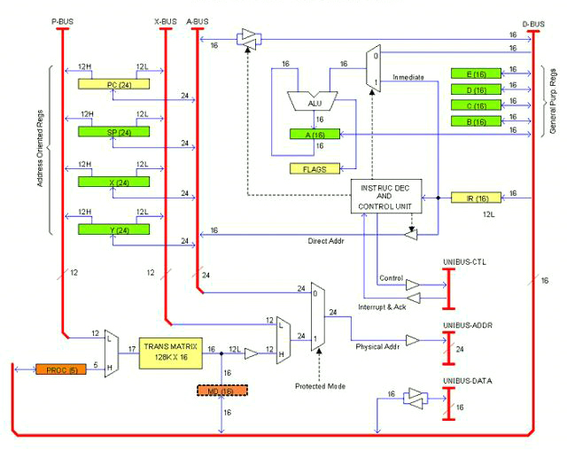
The following drawing is an early sketch (actually the first) of the CPU architecture or block diagram, whatever you want to call it.
This is supposed to be a single PCB card. As per today I don't know if the computer will take one or more units (enclosures); several cards, for sure. The idea is that all cards (and/or units) will be plugged to a common bus that I have called UNIBUS (as that of the legendary PDP-11, not sure if I'm going to adopt exactly that bus).
The UNIBUS consist of Data lines (16), Address lines (24) and Control lines including IRQs. In the drawing they are termed: UNIBUS-DATA, UNIBUS-ADDR and UNIBUS-CTL respectively. This is the way out for the unit (or Card).
There are also internal buses. Those are: D-BUS (16 bits Data), A-BUS (24 bits Address), X-BUS (12 bits Offset) and P-BUS (12 bits Page). These buses communicate registers and other resources inside the CPU card.
Registers can be classified into three categories:
- General Purpose: A, B, C, D, E
- Address Oriented: PC, SP, X, Y
- CPU specific: IR, FLAGS, PROC, MD
There is also the Trans Matrix.
General Purpose registers are 16 bits and they are accessible to the applications programmer. The Accumulator (A) serves as left operand and result holder for the ALU (as in must real-life processors).
Address Oriented registers are 24 bits. They have bidirectional access to the A-BUS and split one-way access to the P-BUS and the X-BUS. In the drawing, each line is marked with the number of bits it carries; when split, an H or L suffix added to the number indicates whether it is the Most or Least significant half.
CPU specific registers have different sizes. IR (16 bits) is the Instruction register; FLAGS is the Status register. When the CPU is in Protected mode, the register PROC (5 bits) indicates the current process number. MD is a fictitious register that represents the current Matrix entry.
The Matrix is a SRAM arrangement of 128K rows by 16 bits. It is addressed by the combination (multiplex) of PROC and the P-BUS. The 12 least significant bits of the selected row represents the physical base address of the Page Frame to be addressed in the current bus cycle. By multiplexing this output with X-BUS (which contributes the Offset) the whole 24 physical address is obtained. If the CPU is in Protected mode, that address is taken to UNIBUS-ADDR; otherwise, the A-BUS content is taken instead.
In the drawing, registers are marked with different colors to highlight privileged use. Green registers are accessible to the Applications programmer. Orange registers are only accessible to System programmers (that is, if the CPU is in Protected mode, code cannot access these registers if it is not in page frames flagged as "Supervisor"). Yellow registers are indirectly accessible throughout instructions; for example, a jump instructions overwrites the Program Counter. When the CPU is in Real mode, page priviledges are not checked so orange registers are accessible to all code.
Note that register PROC is for System programmers use. That is the way for Kernel code to work in Super-Linear space (I'm keeping my idea of the Kernel working in Protected mode but this may change).
Some implementation details are not clearly illustrated in the drawing as for example the rules for transferring data between registers of different sizes. There is a number of different ways of doing that but I'm not going to work it out at this time.
|
Homebuilt CPUs WebRing
JavaScript by Qirien Dhaela
Join the ring?
David Brooks, the designer of the Simplex-III homebrew computer, has founded the Homebuilt CPUs Web Ring. To join, drop David a line, mentioning your page's URL. He will then add it to the list.
You will need to copy this code fragment into your page.
Project start date: May 13 of 2009
|