ContentThese notes are for my own use. You can read them, of course, but don't expect them to be so usefull.
ISSUES
Loading a register that is being used as a pointer
I staked with a simple data-transfer philosophy in which there is always a SOURCE register and a DESTINATION register. If transfer occurs from or to memory then the SOURCE or DESTINATION register (respectively) provides the address; this is the case of the PC, the SP or any register used as a pointer in an Indirect Addressing instruction.
Following this simple philosophy, I am negated to latch the Address Bus content to a so called "Memory Address Register" (MAR). Instead, I am planning to provide the Address directly from SOURCE or DESTINATION registers.
This seems to work pretty well (on paper, at least) except for the particular case in which the SOURCE and the DESTINATION registers coincide. That is the case of restoring the SP content directly from the Stack or loading any register by using itself as a pointer (Ex: LDX B, B).
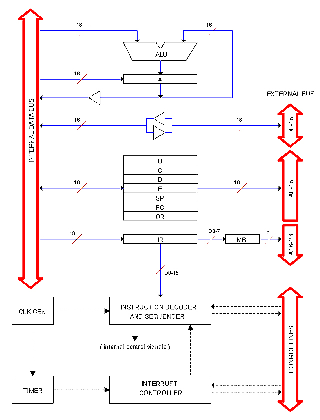
To understand the issue, lets see what happen during a normal Indirect Address instruction such as LDX A, B (see CPU Block Diagram above).
This instruction tells the CPU to load A from the memory location which address is the content of B. Here, A is the DESTINATION register and B is the SOURCE providing the memory address.
For executing this instruction, the CPU will open the B register to the Address Bus, then it will activate the BUS RD signal and finally it will signal A to latch whatever is in the Data Bus.
Now lets "run" the problematic instruction: LDX B, B.
This instruction will execute the same way: Register B will open its buffer to the Address Bus to provide the address; then the BUS RD signal will be activated and finally the same B register will be signaled to latch the Data Bus content.
Problem here is that, as soon the content of B changes, so the address, which will cause the data bus to change unexpectedly causing data corruption.
 Possible Solutions Possible Solutions
There is a number of ways to solve this problem. The simplest one is to forbid Indirect Addressing over the same register. This may be convincing specially because pointing a register with itself does not seems very useful in the first place.
Another solution is to always latch the Address Bus content using a MAR register as most computers do. But I don't want to because it will defeat my data-transfer philosophy all together. A more convincing argument for not to use a MAR register is the delay penalty it would impose to every bus cycle.
There are still more solutions. For instance, I can use the OR register only for those problematic cases. During indirect addressing instructions register OR is not used.
The definite solution is still pending but we can see that the simple data-transfer philosophy I staked on have not been defeated yet.
Issue Resolved
I will simply forbit indirect addressing over the same register used as a pointer. For instance, the follow instruction is illegal:
LDX B, B ; Load register B from memory location which address is the content of B.
Illegal statements of this kind have two consequences: (1) The Assambler will generate an error. (2) The CPU will generate an exception.
Interrupts and the Memory Bank register (MB)
I have established that "vectors" in Heritage/1 interrupts are nothing but the actual ISR address. The reason for this dangerous scheme comes from the count of 64K interrupt "vectors" which in turn comes form the Data Bus size. 64K is too big for a real interrupt vector so I opted to make it a memory address.
But there is a problem with the Memory Bank register (MB): If a program that had switched the MB is interrupted, then the address supplied from the interrupter device will apply to the new bank and not to the intended previous one, so the need for saving the MB register before branching to the new ISR. However, this is not possible in the current architecture because MB is not connected to the D-BUS.
Possible Solutions
One solution is to simply build a path from MB to the D-BUS so we can save/restore the MB register to/from the Stack as we do with the PC. Additionally we can establish that ISRs always reside in Bank 0 so the Interrupt Controller always reset MB before passing control to the ISR.
Another solution is to re-architecture Interrupts. We can opt, for instance, to a "real" 8-bits interrupt vector leaving the remaining 8 bits for setting the MB content.
Issue Resolved
A path between MB and the D-BUS was added. Since MB is 8-bits and the Flags Register (F) is also 8 bits, I resolved to save both at the same time in a single memory (16-bits) before serving an interrupt request.
MISC
Software Development Tools
-- Cross-32 Meta-Assembler, available from Universal Cross Assemblers in Canada
Recommended by: John Doran.
BRAINSTORM
I use this book for making notes about crazy ideas as they come to my mind. I also use the book for discussing less insane ideas with myself. Some people say that talking to your self is not necessarily a sign of illness; problem starts �they say� when you commence to reply your self.
The first HERITAGE/1
These ideas were developed during my first attempt to design a computer targeted to a modern Operating System. That approach was discarded for focusing in a simpler machine with no OS in mind.
Early (very crazy) Ideas
A Linux MiniComputer?
If I managed to write a Linux Kernel that runs on my machine, then it would become a Linux Mini-Computer. Not only it will behave similar to 1970's UNIX machines but it also (and most importantly) will be able to run existing (Open Source) Linux software on top of the Kernel.
I know this is too big for me alone so much likely will never happen... just a crazy idea that came to my mind.
RS232
05/15/2009
A serial (RS232) port. I can't imagine a simplest way of connecting the machine to the outside world. This would be the way for dumping large amount of machine-code directly into memory.
The "multi-little" approach
05/16/2009
This is really crazy. Since modern operating systems such as Linux always try to distribute process among available processors, it occurred to me that I could build a machine using many little microprocessors each of them being capable of handling a user process.
By "little microprocessors" I mean cheap ones, such as the legendary Z80. They lack a "protected mode", indeed, but this were something to be handled by an "arbitror" circuit (anyways needed), not by the processor itself.
Hey, Craig... could you please prove this proposition for me using your so called "Object-Z notation"?
Hardware-isolated Kernel
05/21/2009
I can imagine a computer with two CPUs. But not two identical CPUs but on the contrary, two CPUs that are very different each other.
One (lets calle it "CPU-0") is very low profile whereas the other ("CPU-1") is full featured. Each one has its own separate physical memory; they don't share memory and possibly no storage either; they are totally isolated from each other.
CPU-0 runs the Kernel and it does in "real mode": no virtual memory, no protected mode. As a matter of fact, this CPU does not implement those advanced technologies.
CPU-1 runs the user processes in protected mode; possible this is the only way it can operate: in cannot be "switched back to real mode". The OS Shell also runs in CPU-1 as an ordinary user process. Both Kernel and applications runs concurrently implying that the Kernel never stops: there is no switching between Kernel and User modes.
The only link between the two CPUs (apart from the power supply) is by the mean of hardware interrupt requests. Actually, all processes in CPU-1 runs as IRS routines. The Kernel switches processes by issuing hardware interrupts to CPU-1. Similarly, CPU-1 notifies the Kernel via hardware interrupts. Or maybe there is a "secret path" between the two. We may call it "Inter-Bus" or maybe: "Tunel".
Estrange architecture... Just another idea among many.
Pre-sorted Prefetch
I asked my self how can possible be for a processor to execute every instruction in a single clock and, besides, what is the gain if it will have to fetch the code anyways. The answer is, of course, prefetch and pipelining. Then it occurred to me that I could "easily" implement a prefetch scheme in which code is unmistakable available to the CPU. This is the idea:
There are actually two processors, one into the other. The outer one is in charge of prefetching, nothing else. If my "Trans Matrix" idea holds, then this would be processor who dealed with the Matrix for making address translation and that stuff but this is not important now; the interesting part is how this processor will do prefetch and how is the prefetched storage area.
Well, the prefetch area is actually a stack. The inner CPU (the "real" one) will use its PC as a stack pointer. It simply pops code from the "stack" and executes it right away, no fetch needed. Moreover, the stack itself could be used as IR with no need for a transfer. I will forget about pipelines for now; with just having the code right in place all the time would be a tremendous improvement with respect to the old-fashioned approach I'm taking for the Heritage/1.
So the outer processor (or "preprocessor", as we may call it) needs to make sure that the code is being placed in the right order. So this gay is smart, it knows the instructions set or at least it knows branch instructions.
Knowing this, it will do jumps along its memory reading, following the program flow and making sure the "stack" content is not only prefetched but also "pre-sorted". You may be asking: What about conditional braches? You are right; prefetch prediction is too complicated so the "pre-processor" will simply stop prefetching as soon as it encounter a conditional branch.
Another question you may be asking is about data. Well, in reallity there are two stacks: one for code, the other for data. The computer is Havard inside, Von Neuman outside... something like that.
Well, that is the idea. I know it's not as easy I've said (I know by experience that finding things easy is not a good sign) but I found it cool and wanted to write it down.
Early Design topics
Picturing my old-fashioned Mini-Computer
05/29/2009
I have given a name to her: "MDM-24" for Multi-Dimensional-Matrix, 24 bits address. The internal architecture is more or less defined. But how will she look like from outside? --Like an old-fashioned minicomputer, of course!
The MDM-24 minicomputer is pretty much inspired by the legendary PDP-11. It consists of several rack-mount enclosures (units) interconnected through a common bus called UNIBUS. From outside, the UNIBUS is nothing but multi-pair cables ended with DB37 connectors going from one unit to another in a daisy-chain fashion. Each unit has its own power supply, of course.
The CPU unit distinguishes it self because of the Control Panel in the front with the classical switches and LEDs. Inside is the CPU Card but there are also Memory Cards and possibly others. Apart from UNIBUS connection, the CPU features a RS232 port (DB9 connector) used for maintenance only.
Other RS232 ports (DB9 connectors) are available in the "COMM Unit". Users connect to the computer using "Terminals" attached with serial cables to these ports. Since Terminals don't exist in modern times, users will employ PCs running Terminal emulation programs (such as HyperTerminal) instead. Remote users can also connect through the telephone line using modems as in the old days. Future development will provide Ethernet access to TPC/IP local network; Ethernet cards will also reside in the COMM Unit.
Storage goes separate in the "STORAGE Unit". It can host any sort of storage devices such IDE hard drives, RAIDs, flash, etc. Future development will provide access to USB Memory Sticks and external hard drives; those cards will also reside in the STORAGE Unit.
Other units can be developed in the future to meet specific needs. Also more units of same type (STORAGE for example) can be attached to the computer via UNIBUS. Even more than one CPU would be possible by structuring the appropriate arbitrage mechanism. Modularity at the Unit level (thanks to UNIBUS) is a key principle in MDM-24 design.
Units are also modular. They are basically multi-card frames with the UNIBUS in the back plane. So before producing a new unit, I will probably produce a new card for a existing unit.
Operating the MDM-24
There is no automatic boot up. When the MDM-24 is powered-on, she doesn't do much more than basic initialization of its micro-coded control circuit.
If the purpose is to experiment with low level software, this is the time for doing so. Software can be entered by hand using the switches in the Control Panel. It can also be entered using the CPU RS232 Port dumping large amount of code into selected zones of Memory or even the Matrix. By using the Control Panel, the computer can also be switched to Protected Mode back and forth, ran in single step, etc. This is "debug-time"!
If the purpose is to load the Operating System so the computer can do something useful, the operator has to enter the boot-strap routine manually, either by switches or CPU RS232 Port. The OS should reside in a well known place at the STORAGE Unit.
Once the OS is up and running, the computer can be operated from Terminals (or PCs running Terminal Emulation programs) attached to the COMM Unit (either locally or via modem).
The sake for Concurrency
06/01/2009
The idea of the E-BUS (borrowed from the PDP-11 UNIBUS) makes concurrency almost natural. However, it is not free: one have to plan for it.
I am planning to take advantage of DMA cycles. While the hard drive is transferring bulk data to Main Memory, the CPU could be doing something else, but what? Virtually nothing, because any single thing would require access to memory thus to the bus. The solution is to split the bus into different paths.
This is not new in computer engineering, of course, but I don't want to break the topology that I already have (based on the unified E-BUS). What could I do?
The solution is to keep the E-BUS outside (between units) but not inside (between cards). It occurred to me that the link from cards to E-BUS can be switched. One special card (or maybe a "mother board") can serve as "bus router" making different links between different cards inside the unit and only one of then going to the external E-BUS.
I would have the Main Memory distributed among two cards. While the hard disk is transferring bulk data to one, the CPU is using the other for doing something else.
It's a good idea... I will think about it.
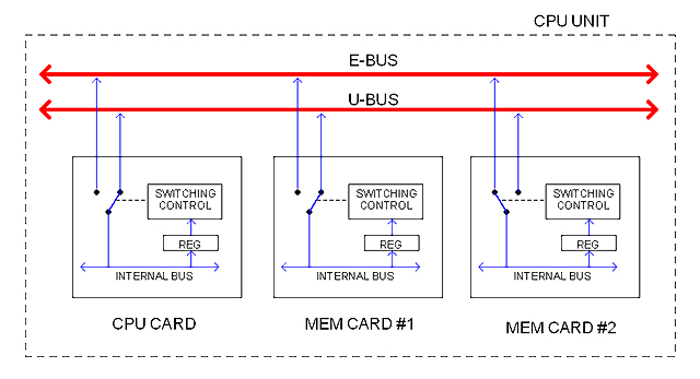
Auxiliary Bus (U-BUS)
I haven't mentioned it but it is obvious (I think) that I don't want to experiment with Pipe Lines, Prefetch, Cache, and that kind of things. No for now at least. So "concurrency" takes me to somewhere else.
The following diagram, for example, illustrates the idea of an auxiliary bus inside the Unit (unit bus or U-BUS) providing an extra path for concurrent processing.
The E-BUS gives access to the external E-BUS whereas the U-BUS provides only internal inter-cards connectivity. All cards would feature the standard ability to switch between the two buses. For doing that, a configuration register (REG) would allow the CPU to dictate the current path status at run-time.
In the diagram, MEM CARD #1 is connected to the external E-BUS possibly getting bulk data from a hard drive whereas the CPU CARD is using MEM CARD #1 for doing something else.
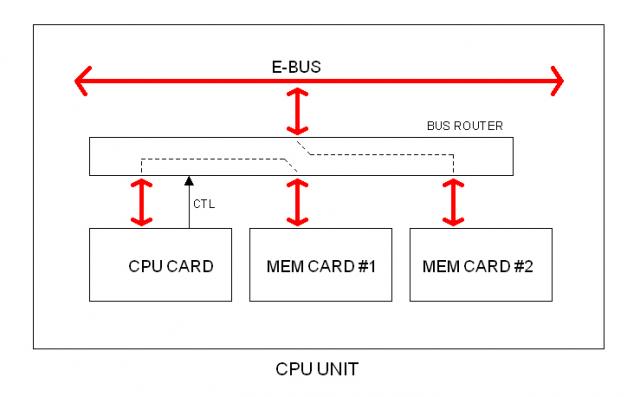
Bus Router
Here is another way for providing the extra path. Cards do not connect to the E-BUS directly but via a BUS ROUTER. This circuit is under the CPU control.
Microcode? Are you sure?
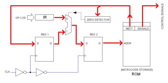
Microcoded FSM
This idea is pretty much borrowed from Bill Buzbee Magic-1 design. It is basically a Finite State Machine (FSM) in which the "next state" (in this case, next microinstruction) is bit-mapped within the microinstruction itself.
As in the Magic-1, the very first block of ROM would contain, one after another, the "first microinstructions" of all instructions so the OP CODE can address them directly. Once the first microinstruction is addressed (from OP CODE), its NEXT field can point to anywhere within the ROM space to continue the instruction sequence.
In address 0 is the HALT instruction which NEXT field is equal to zero. This allows the FSM logic (using the ZERO DETECTOR) to address the ROM from the Instruction Register (IR) rather than from the NEXT field of the current microinstruction.
As per implementation, a detail that I can anticipate is that PROM memories are usually slow (120 ns in contrast with 70ns of typical SRAMs). I have seem 70ns PROMs but they are very expensive. One solution would be to use SRAM instead, being the content dumped from PROM at Power-On time. This is relatively complex due the fact that there is no CPU at Power-On time!
I've been considering a 12 MHz clock because that makes 83 ns cycle, pretty much the typical access time for SRAM chips.
Hard-Wired Intruction Decoder and Sequencer
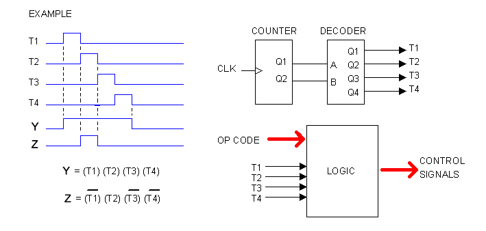
Microcode is not the only way to go. We can also decode instructions by pure (hard-wired) logic, as illustrated below.
Let's imagine that the CPU will take 4 clocks to fetch and execute the longest instruction. Let's imagine also that most instructions contain bit-mapped fields so many control signal derive directly from the instruction itself. In the diagram above, OP CODE refers to just that: the Operational Code (without the bit-mapped fields).
Here, T1, T2, T3 and T4 are actual signals. They are easy to obtain from a counter and a 2-to-4 bits decoder, as illustrated.
The time-diagram on the left is an hypothetical example showing two control signals: Y and Z. Both signals can be represented as products of T1, T2, T3 and T4. This would be for one instruction only; for different instructions, Y and Z will take different products, depending upon the OP CODE, so the equation for each control signal takes this generic form:
Y = (T1) (T2) (T3) (T4) (OP_CODE)
In other words, any control signal can be produced by the mean of a combinational logic which inputs are: T1, T2, T3, T4 and the OP CODE, as illustrated in the diagram.
In practice, OP CODE will not be too wide since the instructions will devote most of their bits to encoded fields, as mentioned before. Control signals, however, will be quite numerous, in the order of 50 maybe. But I suspect that the Logic circuit can be dramatically simplified using those simplification technics we all learned at school.
As per implementation, I suspect that this can be built very easily using a PLD chips (such as ATMEL ATF2210C) rather than discrete SSI/MSI logic.
Considering PLDs (not FPGAs)
It is all about density. If I wanted to build a "pocket computer", I'd surely picked FPGAs. But I want my computer to be bulky, as in the old days. However, employing only SSI/MSI chips would make it "too bulky". That's why I'm turning to what is in between: PLDs, or actually a mix of PLD/SSI/MSI.
Moreover, FPGA portraits important constraints to me. To start with, I'm determined to use the traditional (and cheap) 0.100 inches prototyping boards, so I need all components to come in DIP packages. Adapter boards exist but they are prohibit to my budget and, besides, I don't like them... I mean, I can't stand the vision of my prototyping boards with such an ugly factory-made douther board on top, full of features that I won't use, particuarly that USB connector... no way!
Another problem that I see with FPGA is modularity. Being them so dense, I would be tempted to encapsulate large amount of logic in a single chip. Indeed I can always make changes to the firmware but that is not the kind of "modularity" I seek; it is not being able to start from scratch each time, but instead to be able to change one part without impacting others.
So I started to explore PLDs. ATMEL ATF22V10C, for instance, seems perfect for the "hard-wired" CPU Sequencer that I am picturing: no more, nor less. In other words, PLDs seems to provide the kind of integration level I seek for the Heritage/1.
PREHER-816
After dropping the first Heritage/1 effort, I came with an 8-bits candidate called PREHER/816. That approach didn't last for long.
Memory Banks
64KB of memory should be enough for experimenting with low-level software, even with peripherals mapped in that space. However, we can extend the range by using a Memory Banks scheme.
We can store the Bank Number in a 8-bits hidden register. An instruction maybe termed SETBNK (number) would be employed to switch banks. This allows for 256 banks, that is 16MB of memory.
This could be also exploited as a rudimentary support for protected multi-tasking. If the OS manages to allocate different processes in different banks (64K per process) and development tools (Assemblers, Compilers and Linkers) are designed not to allow SETBNK instruction in "Application Development Mode", then it would be nearly impossible for application code to trespass process boundaries.
As per address lines, the internal address bus (A-BUS) would still 16 bits whereas the external address bus (that in U-BUS) would have 24 lines, the 8 most-significant ones being fed from the BANK register.
Implementing INC/DEC instructions with actual Counter chips
I am considering this idea since Heritage/1. If all registers are built using presettable up/down three-state binary counters, then I can execute INC/DEC instructions in only one clock cycle (T1). This might represent a notable improvement of the overal execution speed since a typical program employs a good deal of time looping through counter variables.
The only problem is cost. Until now, I were thinking of building registers with 74HC374 chips (one chip per 8-bits register, two for 16-bits registers). With presettable counters such as the 74LS169 (and 74HC244 as buffers because this counter doesn't provide three-state outputs) the cost per register may increase by a factor of three.
An alternative is to provide INC/DEC capabilities to only a few registers (i.e. PC, SP and C) leaving the rest not incrementable... or we can increment those others via ALU, in which case we tell programmers (which programmer apart of myself?) to use the register C as a loop counter becouse it is faster.
The final Heritage/1 machine (LAB implementation)
Eventually, the PREHER/816 design evolved into the final Heritage/1 machine.
Memory Banks revised
I'm changing course (once again) toward 16-bits architecture (both Address and Data) so all my registers are now 16 bits wide. However, a Memory Bank register (MB) of 16 bits implies 32 bits of total addressable space which sounds too much for me; I mean, I feel that this would complicate the hardware unnecessarily.
The other thing is software. I should be switching banks by the mean of an instruction such as this:
SET MB (number)
This is equivalent to this:
LD MB, (number)
which is an immediate addressing instruction requiring an operand fetching cycle. So switching the Memory Bank would costs 8 clock cycles: 3 for OP COD fetch, 3 for Operand Fetch and 2 for execution. This might represent too much overhead for an operating system trying to take advantages of the banking support.
I think I can do better by making the MB register 8-bits, which implies a total addressable space of 16 Mwords (32 MB) which is more than enough. This would allow me to embed the MB content (bank number) within the 16-bits instruction code.
Now the instruction SET BANK would execute in just 2 clock cycles (5 total with the op cod fetch) which is much faster when accumulate over thousands of iterations per second.
The use of small cards forces extensibility strategies
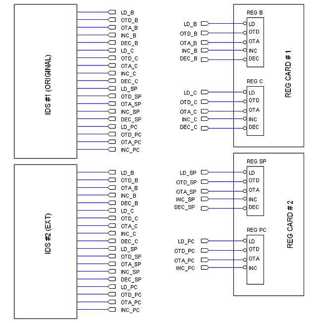
The prototyping boards I ordered are relatively small (5.5 x 8 inches) so chances are for some circuits to expand among several cards. This is particularly likely for Registers and the Instruction Decoder and Sequencer (IDS).
Actually I am not unhappy with this reality; on the contrary, what if I wanted to implement more instructions in the future? The natural way would be to develop some kind of "IDS Extender" card. In this sense, the fact that the first IDS card were extensible from day one represents an advantage rather that a disadvantage.
Problem here is the big amount of connections between the IDS and the register cards, so the goal is to implement extensible IDS cards in an elegant, ordered fashion.
Here is the scenario:
The original IDS card (IDS#1) provide all control signals for the two register cards; later on, a second IDS card (IDS#2) is developed to provide more instructions. But the new instructions control the same registers so the new card provides exactly the same control signals. Question is how to interconnect all those wires without making a mess.
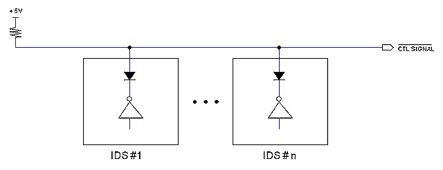
One possible solution is to wire all control signals in a bus so I can connect as many IDS cards as needed, as illustrated bellow.
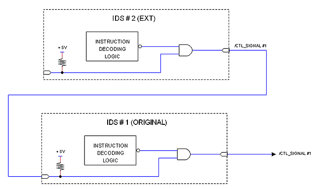
Another solution is to conceive the second card as an extension that connects to the first card only; a third card could be connected to the second and so on. The following figure illustrates the idea.
This arrangement is simple and natural but presents some problems. One is the delay introduced by the AND gates; the other has to do with pins count: Control signals are expected in the order of 70 and now pins would be doubled for each IDS card.
Cards names
Examples:
H1-REG1-1 ; Registers card number 1, version 1
H1-REG2-1 ; Registers card number 2, version 1
H1-REG2-2 ; Registers card number 2, version 2 (replaces previous one)
H1-ALU-1 ; ALU, version 1 (only one card needed for the ALU)
H1-ALU-X1-1 ; ALU extension 1, version 1 (The ALU was extended later with more functions)
H2-ALU-1 ; Heritage/2 ALU card !
Diodes-Matrix as ROM memory
In principle, Memory (RAM/ROM) should not be placed in the CPU Unit; a dedicated unit should be used instead. The "problem" here is that, using today's technologies, Memory will fits comfortable in a single card, so placing that only card in a unit would be a waste. I'm aware of that I'm seeking a justification to make things primitive and inconvenient, but I really wish to make my computer to look similar to those of the 70's.
So making a primitive, bulky ROM Memory with diodes has no other objective but to justify the use of a dedicated Memory Unit. It would be a card full of diodes; it could be "programmed" via jumpers: one jumper for each matrix node. The card would also contain decoders, buffers and some other logic.
This kind of memory would be perfect for storing a "Loader" (bootstrap) program so the operator don't have to enter it from the Control Panel switches. Diagnostic programs would also fit. I could even interchange different programs by just interchanging cards. It would be fun.
I will seriously consider this idea among others... such as using magnetic tapes as storage !
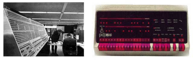
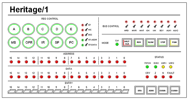
Control Panel
7/8/2009
Computer Control Panels have gradually simplified along history. 1950's main frames featured large panels full of lamps monitoring any single bit from the computer interior. 1970's minicomputers, in contrast, had a minimum of switches and lamps devoted mostly for entering and debugging programs in core memory.
This observation is both guiding and confusing my design of the Heritage/1 Control Panel. What exactly will I want to do from that panel apart from entering code? Debugging circuits? Watching the progress of my software in great detail down to the control signals themselves? I mean, will I want to enter individual control signals manually from the Control Panel?
I were planned to build a "BUS LAB" for that kind of "intimate debugging"; that would be a separate development tool to use during the development of the Heritage/1, that is, before the machine actually existed. But, what about to combine the two functionalities together to come with the definite Control Panel design with "intimate debugging" capabilities?
One option is to build a large panel such as that on the IBM 360 but that would be too glamorous, I think, and quite expensive too. Another option is to group functions together in the aim of saving space and resources; for example, I can place one single set (switches and LEDs) for all registers, with a register-selector key.
The other point of attention is wiring. Where exactly this control panel would be within the CPU circuitry? The natural position, I think, is in place of the Instruction Decoder and Sequencer (IDS), that is, when the computer is in "Debug Mode", the IDS is defeated and the Control Panel takes over.
This vision is very helpful when it comes to design the wiring. I am considering, for example, a "Bus Controller Card" located in the Backplane itself (not actually plugged to it). In "Normal Mode", IDS cards are connected to the buses in the Backplane; in "Debug Mode", the Bus Controller ignores signals coming from IDS cards and connects the buses to those signals coming from the Control Panel instead. As per wiring, the Control Panel would be connected directly to the Bus Controller by mean of a long ribbon cable, being the Control Panel itself located somewhere else.
As per monitoring (LEDs), I don't really need to monitor registers individually but just the Internal Data Bus. When the computer is in "Debug Mode", opening a register buffer momentarily to the internal bus will be enough for watching the register content. This will save a lot of wires and chips. Maybe some important registers such as the PC will worth their dedicated LEDs, as well as those that don't connect to the Data Bus such as the MB (Memory Bank) and other "hidden registers".
This simple but debug-capable control panel could be something similar to this:
Concatenating instructions
I have imposed to my self a 6-clocks limit for the longest execution time. Problem is that the CALL instruction has exceeded that limit because it needs to save the Program Counter to the stack before doing the branch. Also, instructions PUSH and POP have resulted kind of odd because they basically do normal memory accesses (T1, T2, T3) preceded by SP increment or decrement, so the memory access cycle would occur at times T2, T3, T4 which is not "normal".
I see, however, that instructions of that kind appear to be concatenations of simpler instructions, so why not to do just that: to concatenate simple instructions for making complex ones?
Let's see what we can do.
In the Heritage/1, any instruction finishes execution by activating the signal SF (Status Fetch). This signal is used for clearing both the IR and the Instruction Sequence Counter to enforce an Op Code Fetch with the next clock cycle. To concatenate instructions A and B we only need to replace the IR output with the B op code while still generate FS signal to clear the Sequence Counter. But, where instruction B will reside? Not in RAM, not in ROM, but hardwired (with actual wires, not even diodes) behind a MUX that select between this "instruction" and the IR output. Instruction B will finish as normal so next clock cycle after execution will be a normal Fetch.
I think it works.
It may work but not that way
Using a MUX is a perverse idea. I drafted the circuit and it was truly ugly.
The final solution (I hope it is "final") is very different. First of all, the signal SF is not activated by instruction decoding circuitry; what they do instead is to clear both the IR register and the T-COUNTER. Another circuit called "Fetch Sequencer" reacts to the IR=0 condition by activating the SF signal so IDS inhibit themselves and producing the Fetch Sequence on its own.
Concatenating instructions is still valid, but not in the way described in previous note. Instead, different "class instruction decoder circuits" will be selected one after another to conform the chain. I will explain this later in a serious note.
As per instruction cycles, I recently realized the meaning of "machine cycle" so the need for counting time the way most computers do. So I defined the following "cycles counting": T1, T2, T3, T4 for Op Cod Fetch (T4 is for incrementing the PC); T1, T2, T3, T4 for Operand Fetch, and T1... etc. for Execution.
According to this, the fastest instruction in Heritage/1 will take 5 clock cycles (including Op Cod Fech); the longest will take 12. Using a System Clock of 8 MHz (just an example) this makes an average speed of one million instructions per second... on paper at least.
I want to mention that this figure is very realistic because I am not using microprogrammig, so when I say "one clock cycle", I refers to the electrical clock period: 125 ns for 8 MHz.
Managing Fault Conditions
I started to suspect that my scheme for managing exceptions (or Fault Conditions as I prefer to call it) is too limited. It is basically an "OR" of failure signals coming from different circuits merging in a single interrupt line to the Interrupt Controller. With such implementation, an OS handling Fault Condition will be able to recover from errors but not to identify what actual error has occurred.
A richer approach
The very first interrupt vectors (say for instance 0 to 15) are reserved for CPU internal interrupts. One of them (probably 0) is for the Timer, the rest is for reporting Fault Conditions. Being vectors, they have priorities so at design time I would assign higher priorities to worse conditions.
As per wiring, this approach is more natural since different fault conditions come from different circuits in the form of different wires. The Interrupt Controller will be receiving these wires as internal IRQ lines.
Now, an OS handling Fault Conditions will be able to identify the origin of the failure. Still software interrupts can simulate both timer and fault interrupts by using 0 to 15 as the argument.
Illegal instructions
Some instructions are explicitly illegal. That is the case of loading a register from memory using the same register as a pointer (Ex: LDX B, B). This can be handled in three different ways:
1.- The operation is not prevented but it could lead to unexpected result, very difficult to debug.
2.- The CPU detects it and refuses to obey (ignores it) but no Fault is raised.
3.- The CPU detects it and raises a Fault Condition.
Choice #1 is simpler and not as catastrofic as it seems because we can rely on development software (Assembler, Compiler) to handle the error at compiling-time.
Choice #2 is more difficult because the CPU needs to detect the condition. Onces the condition has been detected, simply ignoring it is not a bad thing: as a matter of fact, any "non-code" number used as a Instruction Class (upper 4-bits of the instruction) will be ignored any way since there is no circuit for decoding it.
Choice #3 has the same difficulty as #2. Once the illegal code has been detected, raising an interrupt is not big deal.
The real problem is into detecting the bad code because the the CPU must know the code in advance. It should keep some kind of table to compare. However, I cannot afford to employ time for looking up a table foe each single fetch cycle.
An alternative would be to implement the detection with combinational logic located in IDS cards (since they "know" the instructions better). The premise is to do this without adding time cost.
For now, I'll vote for Choice #1: To handle illegal code at Compiling-Time instead of Run-Time.
Considering �micro-dioded� logic
10/12/2009
Althogth I've discarted microprogramming from the very begining in favor of hardwired logic and the entire design have been built arround such desition, I've been always tempted with the idea of a diodes matrix as a �sequence encoder�.
Dioded matrix is a very old technique employed in 1st. and 2nd generation of computers (that is from 1940's and 1950's) and used extensibly among time not only for computers. It is, then, a technique for which I feel a profound respect.
The only problem with diodes matrix is the physical size. I've found, however, that I could use small matrixes for specific circuits as opposite of a centralized �microcode storage�. Small diodes matrix distributed among circuits in different cards (as planned for hardwired logic) would help to simplify implemention and also so save both board space and money.
I'm not sure if that could be considered �microprogramming�. I hope it would not. But I think it worth to give it a chance. The first step would be to test it at high frequency and see what the waveforms look like.
02/05/2010
It proved problematic, so I discarded. See link below:
http://www.armandoacosta.com/cpu/index.php?branch=447
Control Panel sequences
10/19/2009
When the computer is in Programming Mode, the Control Panel needs to run sequences for reading and writing from/to Main Memory.
The Heritage/1 is a sequential synchronous machine. This means two things: (1) every data transfer within the machine is synchronous with respect to a central Clock (signal CLK), and (2) sequences are synchronous with respect to a central Counter (signals ET0, ET1).
The Control Panel is an exception to this rule when the machine is in Debug or Programming mode. That is because the Control Panel must be the "ultimate resource" when things go wrong, so it cannot rely on any circuit (such as IDS) used for normal operations that, because of its complexity, is more suitable for failures that the Control Panel itself.
This is one reason. The other is the nature of "modes" in the Heritage/1. Debug or Programming modes apply when the computer is in Halt. In that condition, the Time Counter (T-Counter) is frozen at T1 (ET0=ET1=0) which warranties controllers (others than the Control Panel) can not run any sequence. When the computer is in Halt condition, only the Control Panel can take control, so the most natural thing is that it utilize independent means for producing the sequences it require.
TEST Board
11/22/2009
I recently removed the "static debug capabilities" from the Control Panel, one of the key features that Heritage/1 was intended to provide. Now, I have no way (from the Panel) to debug the machine's hardware statically.
The main argument in favor of the removal was that a real life machine would not need it since such kind of debuging is normally done at the factory, not at the field.
Now it occurred to me that I could still ofering the feature but not to the "machine's owner" but to the "manufacturer", and not as part of the Control Panel (from which it was removed) but in the form of a TEST BOARD.
NOTE: The reader shall know that I am both the "machine's owner" and the "manufacturer" but that is part of the fantacy of this project.
The TEST BOARD takes the place of the Master Controller Card (MC). I mean, I remove the MC card, then insert the TEST BOARD. This is because the MC is the one producing the status signals S0, S1 to arbitrate the machine. The TEST CARD would still producing S0, S1 in a convenient way so the machine could be managed "statically".
The TEST CARD would feature push buttons and LEDs on the visible edge, accesible from the CPU frame's front once the cover had been removed. The ingeneer will use those to monitor and activate individual CPU control signals for "static" debugging.
A Harvard Processor
These are the basics of an idea that I just came with for controlling Heritage/1 peripherals in the future.
Heritage/1 peripherals
As mentioned in previous notes, Heritage/1 will treat peripherals as memory cells: each peripheral will share a portion of the main memory that it will utilize as a buffer for transferring data.
This concept is powerful in the sense that it give the OS a first level of abstraction since system software won't have to deal with the "low level" tasks associated with filling the buffer from a particular media such as tape. The price to pay for the abstraction is that some "intelligent being" will be required for carrying on the task.
In modern times we'll surely use a microcontroller chip, but that is not possible for Heritage/1 due the "historical constrain" I've imposed to her design. In the old days, a "low profile" computer would be used instead (as IBM did in the 60s with their "channels") but I can barely afford to build one low profile computer: Heritage/1 itself! What to do?
Smart controllers
I guess that some controllers will require nothing but logic circuits; that is maybe the case of an UART. Others, however, will need some intelligence; perhaps disks and printers will fall into this group.
In any case, the amount of resources needed (such as registers and arithmetic units) would not be too large and, for the other part, a dedicated computer (optimized for the task) would be the optimal choice as opposite of a general purpose one.
I can think for instance in a simple 8-bits CPU with an accumulator, a program counter and some other specialized registers (as opposite of general-purpose registers) with an ALU capable of just the few operations required for that specific application.
But must interesting of all is the fact that a Von Newman architecture is far from optimal for this "low profile" smart peripheral controller I thinking in.
Harvard vs. Von Newman
General-purpose machines followed the "stored program" approach since the early days. Code and data share the same addressable memory space, that is, code is taken into the CPU in the same manner as data is.
This is great for general-purpose machines, but the price to pay is the need for fetching the operational code for each instruction of the program, which takes precious bus cycles that obviously impact the overall performance.
For single-task computers (controllers) the program is fixed. We can take advantage of this by storing that program in a separate memory space. Now, the paths for code and data are separate so we don't need to fetch the operational code; we can just decode and execute instructions directly from where they are: each memory location (just to say) acts as the instruction register per se.
I'm thinking in a small program, of course, so by "memory" I mean a diodes-matrix (kind of old-fashioned ROM). This machine would consists of a few circuit boards, one of those being the diodes-matrix where the little control program resides.
Conclusions
Harvard architecture is being used these days for microcontrollers such as Microchip PICs, so I cannot credit my self for the idea... What I'm actually exploring is the adoption of this concept for Heritage/1.
It would be cool to make the instruction set compatible with that of Heritage/1 (a sub-set), so I could use the same development tools (such as the Assembler) for both.
A quarter hardware for a full computer
Here is a funny idea that just came to my mind, no plans for implementing it but, possibly, a way for saving cost and labor to a quarter.
The idea is this: I could redesign the whole architecture to be 4-bits internal, 16-bits external. All registers, ALU etc. 4-bits; internal buses, 4-bits too. External buses, however, are 16 bits, standing behind latches that patiently wait for the address or data to be completed.
All sequences run 4 times longer; for example, an arithmetic operation is done 4-bits at a time. A memory write cycle that normally takes 3 clock periods, now takes 12 (well, actually less than that) because the address must be collected into the bus latches, 4 bits at a time.
Would this computer run 4 times slower? Not necessarily: the clock speed can be increased 4 times! I've design Heritage/1 around a 4 MHz clock; now I would increase to 16 MHz (T=62 ns) which is still comfortable for HCMOS chips, although care would be needed for wiring due to electromagnetic issues.
There are two cool things about this architecture: (1) A tremendous cost cut, and (2) flexible configuration.
In fact: the machine can be designed to easily accommodate different configurations, that is different bus sizes: 8 bits for a character intensive machine, 16 bits for real time applications or modest general purpose computer, 32 bits for precision scientific applications... just to say.
I would call a machine like that: "Heritage-1/4".
Components under consideration
Comparisson LS, HC, F
06/18/2009
---------------------------------------------------------------------------------
74xx00 LS HC F Unit Winner
---------------------------------------------------------------------------------
VOH 3.4 Vcc 2.5 V HC (Output swing)
VOL 0.35 0 0.5 V
- - - - - - - - - - - - - - - - - - - - - - - - - - - - - - - - - - - - - - - - -
VIH 2.0 3.15 2.0 V HC (Input swing)
VIL 0.8 1.35 0.8 V
- - - - - - - - - - - - - - - - - - - - - - - - - - - - - - - - - - - - - - - - -
IIH 0.02 0.0001 0.005 mA HC (Input Loading)
IIL 0.36 0.0001 0.6 mA
- - - - - - - - - - - - - - - - - - - - - - - - - - - - - - - - - - - - - - - - -
Icc 2.4 0.04 6.8 mA HC (Power consumption)
- - - - - - - - - - - - - - - - - - - - - - - - - - - - - - - - - - - - - - - - -
Delay 10 8 3.7 ns F (Speed)
- - - - - - - - - - - - - - - - - - - - - - - - - - - - - - - - - - - - - - - - -
Price 0.29 0.22 0.07 USD F (Jameco 10+)
---------------------------------------------------------------------------------
CONCLUSSION:
HCMOS seems to be the way to go for this project unless a very high speed is needed for some specific circuit in which case (and only for that circuit) I would chose F components instead.
ICs
Note: Prices are from Jameco (buying 10 or more) unless specified otherwise.
--------------------------------------------------------------------------------------------
Part No. Pins Price Delay (ns) Description
--------------------------------------------------------------------------------------------
74HC00 14 0.22 9 QUAD 2-INPUTS NAND GATE
74HC04 14 0.25 11 HEX INVERTER
74HC27 14 0.15 23 TRIPPLE 3-INPUTS OR GATE
74LS27 14 0.49 10 TRIPPLE 3-INPUTS OR GATE
74HC32 14 0.29 12 QUAD 2-INPUTS OR GATE
74F32 14 0.29 4 QUAD 2-INPUTS OR GATE
74HC4078 14 ---- 8 8-INPUTS OR/NOR GATE (Electronic Glod Mine: $0.35)
74LS138 16 0.45 26 3-TO-8 DECODER DEMULTIPLEXER
74F138 16 0.25 6 3-TO-8 DECODER DEMULTIPLEXER
74F139 16 0.25 6 DUAL 2-TO-4 DECODER DEMULTIPLEXER
74HC157 16 ---- 13 QUAD 2-INPUTS MULTIPLEXER
74LS279 16 0.65 QUAD S-R BISTABLE (Electronic Gold Mine: $0.29)
74LS161 16 0.49 30 4-BITS BIN COUNTER W/LOAD AND CLR
74LS169 16 0.89 30 4-BITS BIN COUNTER W/LOAD AND UP/DN
74LS244 20 0.49 15 8-BITS 3-STATE BUFFER
74F244 20 0.07 8 8-BITS 3-STATE BUFFER
74HC244 20 0.22 30 8-BITS 3-STATE BUFFER
74HC273 20 0.29 25 8-BITS REG
74HC374 20 0.35 15 8-BITS REG W/3-STATE OUTPUT
LINEAR
--------------------------------------------------------------------------------------------------
Vendor Part No. Price Description
--------------------------------------------------------------------------------------------------
Digi-Key LM1084IT-5.0-ND 3.13 LM1084 - 5V POS VOLTAGE REG 5A
Digi-Key MIC29500-5.0VWT-ND 8.71 5V POS VOLTAGE REG LOW DROP 7.5A
--------------------------------------------------------------------------------------------------
Pasive
--------------------------------------------------------------------------------------------
Vendor Part No. Price Delay (ns) Description
--------------------------------------------------------------------------------------------
Jameco 1N4148 0.012 4 SWITCHING DIODE
--------------------------------------------------------------------------------------------
Mechanical
--------------------------------------------------------------------------------------------------
Vendor Part No. Price Description
--------------------------------------------------------------------------------------------------
Jameco 206594CG 10.95 Prototyping Board 5.50x8.00 INCH Single Side, Pad per hole
--------------------------------------------------------------------------------------------------
Digi-Key V2011-ND 19.47 Prototyping Board 6x9 INCH 2-Side, Pad per hole (throug)
--------------------------------------------------------------------------------------------------
CPU Backplane Pinout
Data Slots (96-pins connectors)
- - - - - - - - - - - - - -
A B C
- - - - - - - - - - - - - -
1 GND GND GND
2 D0 CTL D8
3 D1 CTL D9
4 D2 CTL D10
5 D3 CTL D11
6 D4 CTL D12
7 D5 CTL D13
8 D6 CTL D14
9 D7 CTL D15
10 L0 L16 L8
11 L1 L17 L9
12 L2 L18 L10
13 L3 L19 L11
14 L4 L20 L12
15 L5 L21 L13
16 L6 CTL L14
17 L7 CTL L15
18 FLT CTL RST
19 CTL CTL CLK
20 SCSZ CTL SCS4
21 SCSN CTL SCS5
22 SCSC CTL SCS6
23 SCSV CTL SCS7
24 A7 CTL A15
25 A6 CTL A14
26 A5 CTL A13
27 A4 CTL A12
28 A3 CTL A11
29 A2 CTL A10
30 A1 CTL A9
31 A0 CTL A8
32 +5V +5V +5V
- - - - - - - - - - - - - -
Signals Descriptions:
DO-15 Internal Data Bus
A0-15 Internal Address Bus
L0-21 Internal Lamps Bus
SCSZ Set Conditional Status Zero
SCSN Set Conditional Status Negative
SCSC Set Conditional Status Carry
SCSV Set Conditional Status Overflow
SCS4 Set Conditional Status 4 (Future)
SCS5 Set Conditional Status 5 (Future)
SCS6 Set Conditional Status 6 (Future)
SCS7 Set Conditional Status 7 (Future)
RST System Reset
CLK System Clock
FLT Fault Condition
CTL Control Signals (Point-to-Point)
Conrol Slots (120-pins connectors)
Except those marked as "PP" (Point to Poin), all signals in Control Slots are conneted into a Bus. Signals marked as CTL (Control) are not designated yet but they will as the design progresses.
- - - - - - - - - - - - - -
A B C
- - - - - - - - - - - - - -
1 GND GND GND
2 IR0 PP IR8
3 IR1 PP IR9
4 IR2 PP IR10
5 IR3 PP IR11
6 IR4 PP IR12
7 IR5 PP IR13
8 IR6 PP IR14
9 IR7 PP IR15
10 CTL CTL CTL
11 CTL CTL CTL
12 CTL CTL CTL
13 CTL CTL CTL
14 CTL CTL CTL
15 CTL CTL CTL
16 CTL CTL CTL
17 CTL CTL CTL
18 FLT CTL RST
19 CCS CTL CLK
20 CSZ CTL CS4
21 CSN CTL CS5
22 CSC CTL CS6
23 CSV CTL CS7
24 CTL CTL CTL
25 CTL CTL CTL
26 CTL CTL CTL
27 CTL CTL CTL
28 CTL CTL CTL
29 CTL CTL CTL
30 CTL CTL CTL
31 CTL CTL CTL
32 CTL CTL CTL
33 CTL CTL CTL
34 CTL CTL CTL
35 CTL CTL S1
36 CTL CTL S0
37 CTL CTL EOE
38 CTL CTL ET1
39 CTL CTL ET0
40 +5V +5V +5V
- - - - - - - - - - - - - -
Signals Descriptions:
IR0-15 Instruction Register Output
CCS Clear Conditional Status
CSZ Conditional Status Zero
CSN Conditional Status Negative
CSC Conditional Status Carry
CSV Conditional Status Overflow
CS4 Conditional Status 4 (Future)
CS5 Conditional Status 5 (Future)
CS6 Conditional Status 6 (Future)
CS7 Conditional Status 7 (Future)
S0, S1 Operational Status
ET0, ET1 Enconded Time (T1, T2, T3, T4)
RST System Reset
CLK System Clock
FLT Fault Condition
CTL Control Signals (Bus)
PP Control signals (Point-to-Point)
Encoded Time:
- - - - - - - - -
ETT ET0 Time
- - - - - - - - -
0 0 T1
0 1 T2
1 0 T3
1 1 T4
- - - - - - - - -
Operational Status:
- - - - - - - - - - - - - - - - - - - -
S1 S0 Operational Status
- - - - - - - - - - - - - - - - - - - -
0 0 Halt
0 1 Fetch
1 0 Execute
1 1 Interrupt being negotiated
- - - - - - - - - - - - - - - - - - - -
|