The first HERITAGE/1These ideas were developed during my first attempt to design a computer targeted to a modern Operating System. That approach was discarded for focusing in a simpler machine with no OS in mind.
Early (very crazy) Ideas
A Linux MiniComputer?
If I managed to write a Linux Kernel that runs on my machine, then it would become a Linux Mini-Computer. Not only it will behave similar to 1970's UNIX machines but it also (and most importantly) will be able to run existing (Open Source) Linux software on top of the Kernel.
I know this is too big for me alone so much likely will never happen... just a crazy idea that came to my mind.
RS232
05/15/2009
A serial (RS232) port. I can't imagine a simplest way of connecting the machine to the outside world. This would be the way for dumping large amount of machine-code directly into memory.
The "multi-little" approach
05/16/2009
This is really crazy. Since modern operating systems such as Linux always try to distribute process among available processors, it occurred to me that I could build a machine using many little microprocessors each of them being capable of handling a user process.
By "little microprocessors" I mean cheap ones, such as the legendary Z80. They lack a "protected mode", indeed, but this were something to be handled by an "arbitror" circuit (anyways needed), not by the processor itself.
Hey, Craig... could you please prove this proposition for me using your so called "Object-Z notation"?
Hardware-isolated Kernel
05/21/2009
I can imagine a computer with two CPUs. But not two identical CPUs but on the contrary, two CPUs that are very different each other.
One (lets calle it "CPU-0") is very low profile whereas the other ("CPU-1") is full featured. Each one has its own separate physical memory; they don't share memory and possibly no storage either; they are totally isolated from each other.
CPU-0 runs the Kernel and it does in "real mode": no virtual memory, no protected mode. As a matter of fact, this CPU does not implement those advanced technologies.
CPU-1 runs the user processes in protected mode; possible this is the only way it can operate: in cannot be "switched back to real mode". The OS Shell also runs in CPU-1 as an ordinary user process. Both Kernel and applications runs concurrently implying that the Kernel never stops: there is no switching between Kernel and User modes.
The only link between the two CPUs (apart from the power supply) is by the mean of hardware interrupt requests. Actually, all processes in CPU-1 runs as IRS routines. The Kernel switches processes by issuing hardware interrupts to CPU-1. Similarly, CPU-1 notifies the Kernel via hardware interrupts. Or maybe there is a "secret path" between the two. We may call it "Inter-Bus" or maybe: "Tunel".
Estrange architecture... Just another idea among many.
Pre-sorted Prefetch
I asked my self how can possible be for a processor to execute every instruction in a single clock and, besides, what is the gain if it will have to fetch the code anyways. The answer is, of course, prefetch and pipelining. Then it occurred to me that I could "easily" implement a prefetch scheme in which code is unmistakable available to the CPU. This is the idea:
There are actually two processors, one into the other. The outer one is in charge of prefetching, nothing else. If my "Trans Matrix" idea holds, then this would be processor who dealed with the Matrix for making address translation and that stuff but this is not important now; the interesting part is how this processor will do prefetch and how is the prefetched storage area.
Well, the prefetch area is actually a stack. The inner CPU (the "real" one) will use its PC as a stack pointer. It simply pops code from the "stack" and executes it right away, no fetch needed. Moreover, the stack itself could be used as IR with no need for a transfer. I will forget about pipelines for now; with just having the code right in place all the time would be a tremendous improvement with respect to the old-fashioned approach I'm taking for the Heritage/1.
So the outer processor (or "preprocessor", as we may call it) needs to make sure that the code is being placed in the right order. So this gay is smart, it knows the instructions set or at least it knows branch instructions.
Knowing this, it will do jumps along its memory reading, following the program flow and making sure the "stack" content is not only prefetched but also "pre-sorted". You may be asking: What about conditional braches? You are right; prefetch prediction is too complicated so the "pre-processor" will simply stop prefetching as soon as it encounter a conditional branch.
Another question you may be asking is about data. Well, in reallity there are two stacks: one for code, the other for data. The computer is Havard inside, Von Neuman outside... something like that.
Well, that is the idea. I know it's not as easy I've said (I know by experience that finding things easy is not a good sign) but I found it cool and wanted to write it down.
Early Design topics
Picturing my old-fashioned Mini-Computer
05/29/2009
I have given a name to her: "MDM-24" for Multi-Dimensional-Matrix, 24 bits address. The internal architecture is more or less defined. But how will she look like from outside? --Like an old-fashioned minicomputer, of course!
The MDM-24 minicomputer is pretty much inspired by the legendary PDP-11. It consists of several rack-mount enclosures (units) interconnected through a common bus called UNIBUS. From outside, the UNIBUS is nothing but multi-pair cables ended with DB37 connectors going from one unit to another in a daisy-chain fashion. Each unit has its own power supply, of course.
The CPU unit distinguishes it self because of the Control Panel in the front with the classical switches and LEDs. Inside is the CPU Card but there are also Memory Cards and possibly others. Apart from UNIBUS connection, the CPU features a RS232 port (DB9 connector) used for maintenance only.
Other RS232 ports (DB9 connectors) are available in the "COMM Unit". Users connect to the computer using "Terminals" attached with serial cables to these ports. Since Terminals don't exist in modern times, users will employ PCs running Terminal emulation programs (such as HyperTerminal) instead. Remote users can also connect through the telephone line using modems as in the old days. Future development will provide Ethernet access to TPC/IP local network; Ethernet cards will also reside in the COMM Unit.
Storage goes separate in the "STORAGE Unit". It can host any sort of storage devices such IDE hard drives, RAIDs, flash, etc. Future development will provide access to USB Memory Sticks and external hard drives; those cards will also reside in the STORAGE Unit.
Other units can be developed in the future to meet specific needs. Also more units of same type (STORAGE for example) can be attached to the computer via UNIBUS. Even more than one CPU would be possible by structuring the appropriate arbitrage mechanism. Modularity at the Unit level (thanks to UNIBUS) is a key principle in MDM-24 design.
Units are also modular. They are basically multi-card frames with the UNIBUS in the back plane. So before producing a new unit, I will probably produce a new card for a existing unit.
 Operating the MDM-24 Operating the MDM-24
There is no automatic boot up. When the MDM-24 is powered-on, she doesn't do much more than basic initialization of its micro-coded control circuit.
If the purpose is to experiment with low level software, this is the time for doing so. Software can be entered by hand using the switches in the Control Panel. It can also be entered using the CPU RS232 Port dumping large amount of code into selected zones of Memory or even the Matrix. By using the Control Panel, the computer can also be switched to Protected Mode back and forth, ran in single step, etc. This is "debug-time"!
If the purpose is to load the Operating System so the computer can do something useful, the operator has to enter the boot-strap routine manually, either by switches or CPU RS232 Port. The OS should reside in a well known place at the STORAGE Unit.
Once the OS is up and running, the computer can be operated from Terminals (or PCs running Terminal Emulation programs) attached to the COMM Unit (either locally or via modem).
The sake for Concurrency
06/01/2009
The idea of the E-BUS (borrowed from the PDP-11 UNIBUS) makes concurrency almost natural. However, it is not free: one have to plan for it.
I am planning to take advantage of DMA cycles. While the hard drive is transferring bulk data to Main Memory, the CPU could be doing something else, but what? Virtually nothing, because any single thing would require access to memory thus to the bus. The solution is to split the bus into different paths.
This is not new in computer engineering, of course, but I don't want to break the topology that I already have (based on the unified E-BUS). What could I do?
The solution is to keep the E-BUS outside (between units) but not inside (between cards). It occurred to me that the link from cards to E-BUS can be switched. One special card (or maybe a "mother board") can serve as "bus router" making different links between different cards inside the unit and only one of then going to the external E-BUS.
I would have the Main Memory distributed among two cards. While the hard disk is transferring bulk data to one, the CPU is using the other for doing something else.
It's a good idea... I will think about it.
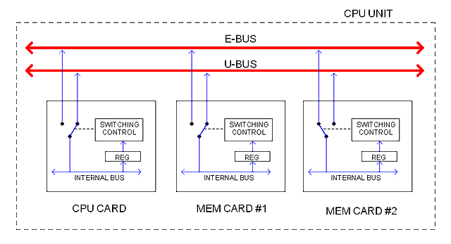
Auxiliary Bus (U-BUS)
I haven't mentioned it but it is obvious (I think) that I don't want to experiment with Pipe Lines, Prefetch, Cache, and that kind of things. No for now at least. So "concurrency" takes me to somewhere else.
The following diagram, for example, illustrates the idea of an auxiliary bus inside the Unit (unit bus or U-BUS) providing an extra path for concurrent processing.
The E-BUS gives access to the external E-BUS whereas the U-BUS provides only internal inter-cards connectivity. All cards would feature the standard ability to switch between the two buses. For doing that, a configuration register (REG) would allow the CPU to dictate the current path status at run-time.
In the diagram, MEM CARD #1 is connected to the external E-BUS possibly getting bulk data from a hard drive whereas the CPU CARD is using MEM CARD #1 for doing something else.
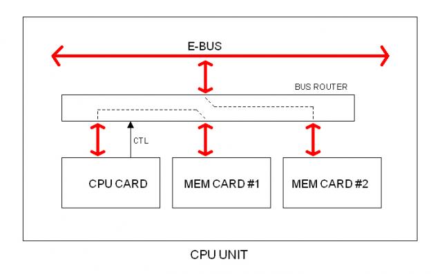
Bus Router
Here is another way for providing the extra path. Cards do not connect to the E-BUS directly but via a BUS ROUTER. This circuit is under the CPU control.
Microcode? Are you sure?
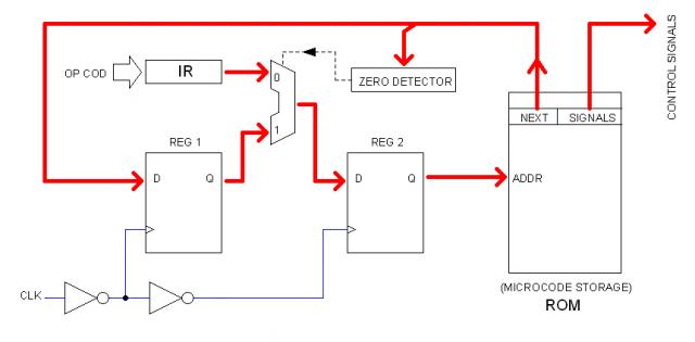
Microcoded FSM
This idea is pretty much borrowed from Bill Buzbee Magic-1 design. It is basically a Finite State Machine (FSM) in which the "next state" (in this case, next microinstruction) is bit-mapped within the microinstruction itself.
As in the Magic-1, the very first block of ROM would contain, one after another, the "first microinstructions" of all instructions so the OP CODE can address them directly. Once the first microinstruction is addressed (from OP CODE), its NEXT field can point to anywhere within the ROM space to continue the instruction sequence.
In address 0 is the HALT instruction which NEXT field is equal to zero. This allows the FSM logic (using the ZERO DETECTOR) to address the ROM from the Instruction Register (IR) rather than from the NEXT field of the current microinstruction.
As per implementation, a detail that I can anticipate is that PROM memories are usually slow (120 ns in contrast with 70ns of typical SRAMs). I have seem 70ns PROMs but they are very expensive. One solution would be to use SRAM instead, being the content dumped from PROM at Power-On time. This is relatively complex due the fact that there is no CPU at Power-On time!
I've been considering a 12 MHz clock because that makes 83 ns cycle, pretty much the typical access time for SRAM chips.
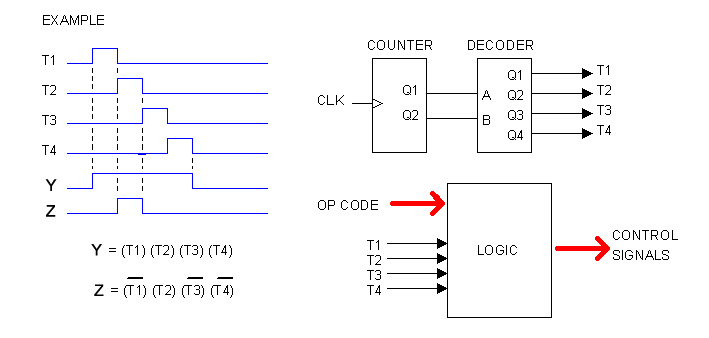
Hard-Wired Intruction Decoder and Sequencer
Microcode is not the only way to go. We can also decode instructions by pure (hard-wired) logic, as illustrated below.
Let's imagine that the CPU will take 4 clocks to fetch and execute the longest instruction. Let's imagine also that most instructions contain bit-mapped fields so many control signal derive directly from the instruction itself. In the diagram above, OP CODE refers to just that: the Operational Code (without the bit-mapped fields).
Here, T1, T2, T3 and T4 are actual signals. They are easy to obtain from a counter and a 2-to-4 bits decoder, as illustrated.
The time-diagram on the left is an hypothetical example showing two control signals: Y and Z. Both signals can be represented as products of T1, T2, T3 and T4. This would be for one instruction only; for different instructions, Y and Z will take different products, depending upon the OP CODE, so the equation for each control signal takes this generic form:
Y = (T1) (T2) (T3) (T4) (OP_CODE)
In other words, any control signal can be produced by the mean of a combinational logic which inputs are: T1, T2, T3, T4 and the OP CODE, as illustrated in the diagram.
In practice, OP CODE will not be too wide since the instructions will devote most of their bits to encoded fields, as mentioned before. Control signals, however, will be quite numerous, in the order of 50 maybe. But I suspect that the Logic circuit can be dramatically simplified using those simplification technics we all learned at school.
As per implementation, I suspect that this can be built very easily using a PLD chips (such as ATMEL ATF2210C) rather than discrete SSI/MSI logic.
Considering PLDs (not FPGAs)
It is all about density. If I wanted to build a "pocket computer", I'd surely picked FPGAs. But I want my computer to be bulky, as in the old days. However, employing only SSI/MSI chips would make it "too bulky". That's why I'm turning to what is in between: PLDs, or actually a mix of PLD/SSI/MSI.
Moreover, FPGA portraits important constraints to me. To start with, I'm determined to use the traditional (and cheap) 0.100 inches prototyping boards, so I need all components to come in DIP packages. Adapter boards exist but they are prohibit to my budget and, besides, I don't like them... I mean, I can't stand the vision of my prototyping boards with such an ugly factory-made douther board on top, full of features that I won't use, particuarly that USB connector... no way!
Another problem that I see with FPGA is modularity. Being them so dense, I would be tempted to encapsulate large amount of logic in a single chip. Indeed I can always make changes to the firmware but that is not the kind of "modularity" I seek; it is not being able to start from scratch each time, but instead to be able to change one part without impacting others.
So I started to explore PLDs. ATMEL ATF22V10C, for instance, seems perfect for the "hard-wired" CPU Sequencer that I am picturing: no more, nor less. In other words, PLDs seems to provide the kind of integration level I seek for the Heritage/1.
|