The Computer
Heritage/1 is a homebrew minicomputer featuring an architecture similar to those of the 1960's and 1970's. It uses the 74HC series of SSI/MSI integrated circuits. It also uses SRAM chips being those the only LSI ones employed. Not even ROM chips has been considered in the design althougth some little programs may reside in "read only memory" made out of fast-switching diodes, that is a (manually programmed) diodes-matrix.
Most registers in this computer are built using presettable up/down synchronous counters. This allow registers to be incremented or decremented in a single clock period without data transfer or ALU usage involved. General purpose registers are also double-buffered so they can write to either Data or Address bus making indirect addressing very simple.
The computer is strictly 16 bits meaning that Memory is organized into words, not bytes. The 16-bits Address Bus can directly address up to 64 Kwords of memory (or 128 KB if you prefer to count it that way).
Instructions are decoded by hardwired logic, that is using boolean algebra instead of microprogramming. This is both interesting and eficient.
A Timer circuit provides a "computer tic" to produce a cylclic interrupt. This may be used by an operating system for scheduling different processes in a multiprogramming fashion.
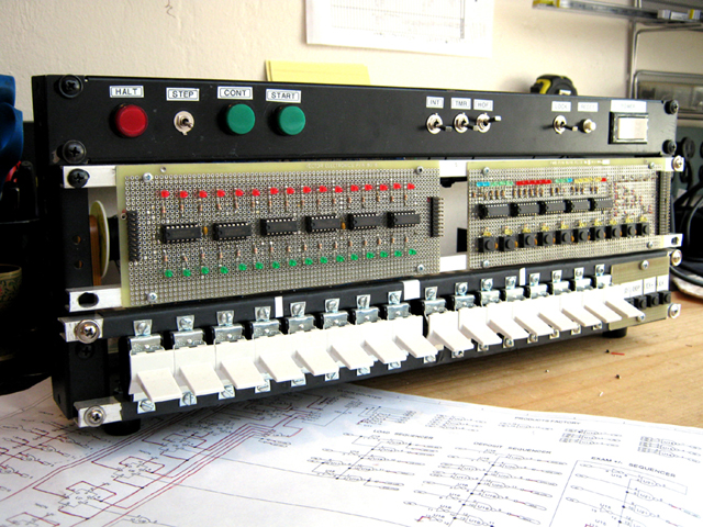
Construction
The Heritage/1 minicomputer will consists of several rack-mount "units" such as the CPU, the Memory Unit, the Comm Unit and others, housed in a 19-inches industrial rack possibly 20RU high. An external bus called U-BUS connects all units together whereas each of those possess its own specific internal bus.
The CPU in particular is housed into a multi-cards frame. Cards are built using 8x5.5 inches prototyping boards that plug to the frame's Backplane.
The CPU Backplane consists of 96-pins and 120-pins DIN 41612 connectors conveniently wired into different interal buses. Some complex circuits such as the Instructions Decoder and Sequencer (IDS) expand among several cards.
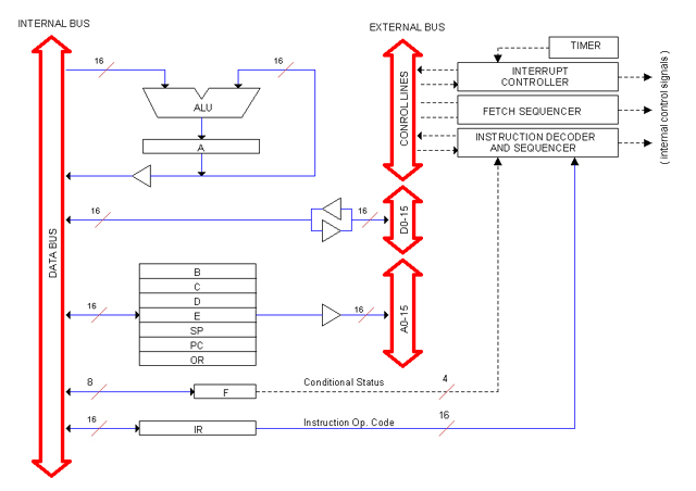
CPU Block Diagram (simplified)
Summary
Data Bus : 16 bits
Address Bus : 16 bits
Main Memory : Up to 64 Kwords
Arithmetic : Signed integer (two's complement)
Inst. decode method : Hard-wired logic
General Purpose regs: B, C, D, E: 16 bits double-buffered to Data and Address buses
Special Registers : A, PC, SP : Accumulator, Program Counter and Stack Pointer
Hidden Registers : IR, OR, F : Instruction Reg, Operand Reg and Flags register
Console Registers : LAR, LDR : Lamps-Address and Lamps-Data registers
Real-Time Timer : 1 ms "computer tic".
Peripherals : Memory Mapped
Interrupts : 64K External Interrupts plus 256 vectored Internal Interrupts
Technology : SSI/MSI HCMOS chips
Construction : Prototyping boards housed in rack-mount multicard frames.
Clock Speed : 4 MHz
Addressing Modes
Register : Data is contained in given register.
: mov a, b ; A=B
Immediate : Data if given in the word following the op. cod (operand).
: movi a, data ; A=data
Direct : Data is in the memory location which address is given in the word following the op. cod. (operand).
: ld a, addr ; A=[addr]
Indirect : Data is in the memory location which address is contained in a register used as a pointer.
: ldx a, d ; A=[D]
Relative : (Branch only). Jump to OFF_SET relative to current instruction address. The OFF_SET if given as an operand.
: jnzr OFF_SET ; PC=PC+OFF_SET
Relative Indirect: (Branch only). The OFF_SET is the content of given register.
: jnzrx d ; PC=PC+d
Stack : Data comes from the Stack which is always pointed by register SP.
: pop a ; A=[SP]; SP=SP-1
Interrupts
The Heritage/1 interrupt architecture allows for 64K interrupts which priorities are determined by the hardware topology. Three control lines are present in the External Control Bus: IRQ (Interrupt Request), IAK (Interrupt Acknowledge) and ISE (Interrupt Services End). These lines are connected to all devices in a Daisy Chain fashion so any interrupter device can open the lines to avoid further propagation along the chain. This way, priority gets establiched by the "proximity" of the device to the CPU.
Peripherals
We call "peripheral" to any device that is external to the CPU. Included in this group are: the Main Memory, the COM Ports, the Tape Drive Controllers and many others. All of them are mapped within the same addressable space.
Some peripherals (notably, Terminals) connects to the CPU via RS232 ports. Most others, however, are attached to a common external bus that we call "U-BUS" consisting of 16 data lines, 16 address lines and 7 control lines.
Peripherals contain their own memory chips allocated in designated addresses. These are wired as dual-port memory so both the CPU and the peripheral circuitry can read/write from/to them. Typically, a status register and at least one-word data buffer are implemented per peripheral.
A typical communication between the CPU and a device runs like this:
The CPU sends a command to the device by writing the device's status register. For the CPU prospective it only had wrote a word to a memory cell. The CPU does not wait for the response but it keeps working on something else.
The Device reacts to the command doing some work. Say for instance that it gets data from the magnetic tape to fill in its internal Buffer.
When the Device finishes, it interrupts the CPU which, in response, reads the Device Buffer into Main Memory. Possibly this cycle repeats several times until the desired amount of data is read into Main Memory.
|