Master Controller Unit (MC)
The mission of the MC is to provide the intelligence to the system. This unit contains the microprocessor (Zilog Z80), the first 24 KB of memory (8KB EPROM + 16KB RAM), and logic for coordinating INT and DMA requests asserted by external devices throughout the EXT-BUS.
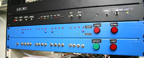
A DSUB-37 connector is present in the rear to expose the EXT-BUS being this the only way out for the MC. In the front, a "traditional" Control Panel (Console) is offered to the Operator for machine control and software debugging.
Operational Modes
The LC-81 minicomputer operates in two distinct modes: Halt and Run.
After power-on or reset, the machine falls into HALT mode. This is accomplished by asserting a BUSREQ to the microprocessor. Since the Console Controller does not depend on software to operate (except for the START button) it can take control of the buses (both internal and external) so this is the time for the Operator to make use of the Console for inspecting/changing memory content (both private and external) as well as peripheral registers.
Pressing the START or CONT button causes the machine to enter RUN mode. This is accomplished by removing the BUSREQ to the microprocessor so it can resume execution. The Operator can stop the machine at any further time by pressing the HLT button which causes the machine to enter HALT mode again.
STEP execution is also supported. This is accomplished by synchronizing with the microprocessor signal M1 which activates at the beginning of each Opcode Fetch cycle.
Private Memory
The memory contained into the MC is said to be "private" because it is isolated from the EXT-BUS by the mean of 3rd-state buffers so no external device can gain access to it in any way.
It is possible to build an external Memory Unit to provide "shared" memory. That would be the one used by DMA capable peripherals.
The use of a separate private memory allows for concurrent operations between DMA operations and normal software execution as long as this takes place in private memory.
EXT-BUS Gating
All EXT-BUS lines are behind 3rd state buffers in the MC unit. A "gating" logic is implemented in order to isolate external DMA transactions from Software running in MC private memory (internal buses) so they can take place concurrently. The logic is as following:
The bus is normally "closed" (high impedance state). In this conditions the Microprocessor access private memory and the Console register SAR (I/O address: 01 and 02). If the Microprocessor attempts to access external memory (address beyond 5FFFH) or I/O other than 01 and 02, the bus "opens", the signal BSY is activated in the bus to indicate that condition, and the lamp "BUS" is illuminated in the MC front panel.
A DMA capable peripheral requests bus control by raising the signal BRQ. In presence of this signal, the Bus Gating circuits closes the bus immediately (if it was not closed already). If the Microprocessor attempts to access external memory or I/O, a wait signal is asserted so the Microprocessor waits until the BRQ is dropped. The BSY signal however is not dropped. The operator can recognize this situation because lamps "BUS" and "WT" in the front panel are both illuminated.
Application programs are expected to run in Private Memory utilizing buffers located in External Memory shared with DMA peripherals. Access to those external buffers is negotiated with DMA as explained and the terms of the negotiation favors DMA in order to ensure the success of those (possibly critical) transactions.
DMA peripherals are expected to monitor the BSY signal, not to assert BRQ is it is active, and not to monopolize the bus for a long period of time.
MC Electronics
The MC electronics resides in three separate boards called respectively: CPU board, Console Registers and Console Controller. The first contains the microprocessor, memory, EXT-BUS 3rd-state buffers and logic. The other two supports the Console's functionality.
Console's buttons, switches and "lamps" (actually LEDs) are located within the assembly mounted on PCBs but no electronics other than LED buffers exists outside the three boards mentioned before.
Console Electronics
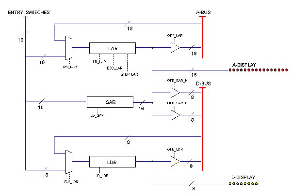
The Console works independently (with no software support, except for the START operation), based in its own logic implemented with discrete TTL components. The circuit is broken into two boards: the Console Controller board and the Console Registers board. The later contains the console's registers, buffers and multiplexers as shown in the block diagram below. The former provides the necessary control signals sequences to manage those resources according to a logic triggered by the buttons and switches available to the operator in the front panel.
In the diagram, A-BUS and D-BUS represent the MC internal Address and Data bus respectively. All control signals (SW_LAR, LD_LAR etc.) are provided by the Console Controller board.
Register LAR (Lamps Address Register) holds the address being presented by the Address lamps. A 3rd-state buffer isolates this output from the A-BUS; control signal OTA_LAR (Output To Address) causes the buffer to open so the content is available in the A-BUS. The input may come from two different sources depending of the state of the preceding Multiplexor: that may be the Entry Switches or the A-BUS; signal SW_LAR determines the Multiplexor state: when active, the Multiplexor switches to A-BUS.
Signal LD_LAR (Load) makes the register to latch the input. Signal STEP_LAR causes the register to increment or decrement its content depending or DEC_LAR being inactive or active respectively.
Register LDR (Lamps Data Register) holds the content being presented by the Data lamps. The input may come from either the Entry Switches or the D-BUS. Buffered output goes to the D-BUS. Control signals SW_LDR, LD_LDR and OTD_LDR (Output to Data) have similar meanings as those in the LAR register. The LDR register, however cannot be incremented or decremented, only latched.
The register SAR (Start Address Register) holds the starting address for the program to be run when the operator presses the START button. Its 16 bits content is read by the Microprocessor into its PC register during a NMI interrupt asserted by the CPU board when the START button is pressed. This takes two reading operations: one for the LSB, other for the MSB, hence two buffers are necessary, triggered by control signals OTD_SAR_L and OTD_SAR_H respectively. These signals are generated by the Console Controller board when I/O ports 01H and 02H (respectively) are addressed by the Microprocessor.
When the operator presses the LOAD button, the status of the Entry Switches is latched in both registers LAR and SAR (signals LD_LAR, LD_SAR). The resulting memory address is read into LDR making the new content visible to the operator in the Data lamps.
When the operator presses the EXAMINE+ or EXAMINE- button, LAR is incremented (or decremented) and the resulting memory address is read into LDR.
Pressing the DEPOSIT button causes LDR to latch the Entry Switches state and that to be written into the memory location (or I/O device) addressed by LAR at that moment. LAR is automatically incremented and the resulting memory location (or I/O) is read again into LDR.
Control Signal sequences to allow all this to happen are built in the Console Controller board by the mean of a diodes matrix. Diodes are pluggable to allow further adjustments in the "microcode" if ever that would be needed.
Schematics
 CPU board CPU board
Console Display board
Console Registers board
Console Controller board
EXT-BUS pinout
|