Back to HERITAGE/1Today (06/29/2009) I decided to make PREHER/816 the main subject of my project. The original "Heritage/1" idea is not longer "putted on hold" but postponed indefinitely so the current design will inherit her name. Why? Because (1) it is an appropriate name, (2) because working on a "pre-project" is quite frustrating and (3) because I wanted to stop the mess of names once an so ever.
So from today on "Heritage/1" refers to the machine I am making now, which is the main and the only one.
BUS LAB
06/29/2009
Before going further, I will build this development tool that I need to test circuits as they come. It is basically a manual signals generator and monitoring tool that will provide control signals (Switches) and will monitor buses status (LEDs). More info in here:
index.php?branch=228
Buying parts for the first time
06/28/2009
Today I ordered parts for the first time in the history of this project. They were 10 prototyping boards from Jameco and some nice (and cheap) switches from Gold Mine Electronics.
I am specially happy with the proto boards because it have been difficult to find good sizes at good prices. This is not particularly cheap (5.5 x 8 inches at $10.95) but is the best I could get and it's not bad at all.
The switches look really nice in the catalog (I hope they are as good) and the price couldn't be better: 59 cents each... I ordered 100 at once!.
The BUS LAB is not designed yet but I need the switches with me before I can make final design decisions. Since switches and other parts need to fit in a panel, physical dimensions count more than one can imagine.
16 Bits: A shine of elegance
06/30/2009
I seemed happy enough with my 8-bit design when suddenly, at mid night, a totally different design came to my mind and I had no option but to jump to my acrylic white board and start sketching the new idea. I don't want to post anything yet other than this little note, until the idea is more mature.
The new architecture for the Heritage/1 is 16-bits both address and data. This means that all registers are 16 bits and implies that any of them can be used as a pointer. This simple fact completely defeats the notion of "data-oriented" and "address-oriented" registers.
Indeed this is nothing new. The PDP-11 was just like that and same approach has been followed by homebrew CPU designers like John Doran.
As per my Heritage/1, I have the following plan:
Except for special registers such as IR (Instruction Register) and MDAR (Operand holder), all regs will be built using counters (74HC169). This allows the CPU to execute INC/DEC instructions in just one clock cycle since no ALU operation nor data transfer is involved.
Not only counters, of course, but 3-state buffers (74HC244) too. Actually, each reg will have two buffers: One to the internal D-BUS (Data Bus) and the other to the external Address Bus. This way each reg can write to either bus. Inputs, however, always come from the D-BUS.
The other change has to do with the instruction decoding mechanism. I'm still determined to use hardwired logic instead of micro-coding (that is for the sake of speed and also because I find it more interesting); however, now that I have a 16-bits instruction (instead of 8) I have room for field-mapping.
This is the idea:
No matter what the data transfer, there are always two registers involved: a source (SRC) and a destination (DES). If data is transferring between registers, that is pretty clear; if it is from or to memory, one register is receiving or sending the data while the other is supplying the address (Ex: PC, SP or any reg used as pointer in a indirect addressing instruction).
So for any data-transfer instruction I only need two fields to say what registers are involved: SRC and DES. For the current design, 3 bits each would be enough, but I will make them 4-bits so I have room for 8 more registers in the future.
After had expending 8 bits in field-mapping, I yet have 8 bits for instruction OP-COD so I can build up to 256 instruction which is more than enough.
And having this reg addresses coded within the instruction I can simplify the logic by using 4-to-16 decoder chips. I will use three of them: One for "data-read" (open buffer to D-BUS) control signals, one for "data-write" (clock registers) control signals, and the other for "address-open" (open buffer to the Address Bus) control lines.
That is basically the idea for the new architecture. I think is elegant and promising. And I hope not to come with a new redesign before this project evolve in a total mess.
Buses, Cards and Backplane
07/06/2009
The problem I have with the BUS LAB is with connectors: not clear on what kind of connectors to use. This concern took me to the CPU buses and connectors but in this case it was different: I could make final decisions about my buses both internal and external, the backplane connectors to use (DIN 96-PINS) and I also could get some idea of how many Cards the CPU might take (about 8).
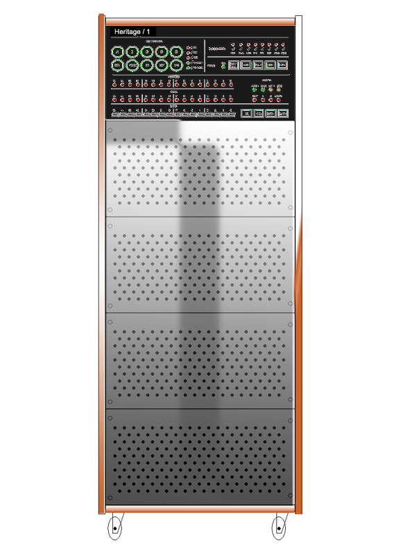
I pictured my cabinet too: a refrigerator-like enclosure, tall and bulky as most minicomputers on the 70's. Now I can imagine the Heritage/1's "body", not just her "spirit"...
As per the BUS LAB, I haven't designed it yet.
Approaching a final design of the Internal Bus
07/07/2009
Looking for standards I got to the VME Bus P1 which utilizes the same 96-PINs connector I chosen. This bus is designed for computers and it designates many power and control lines that I don't need for my Internal Bus, but I decided to adopt the pin out discarding those signals that I don't use but retaining those that I do; these are: 16 Data pins, 16 Address pins, SYS CLK, 8 GND pins and 3 +5V pins. Discounting the rest out, I have 53 extra pins for anything else.
I started wondering if that would be enough for my control signals, that is if my previous forecast of about 70 were currect. In order to approach the answer, I did a detailed signals count over the CPU block diagram. The final pin-count surprised me: only 46.
Of course, in practice they will be more and there will also point-to-point connections between certain cards. But it still makes sense to consider the 53 extra pins for a possible "control signals bus".
Taking shape
07/09/2009
Heritage/1 starts to take shape. I have a very clear idea about the Buses both internal and external, and specially how to build the CPU backplane, how to connect it to the External Bus and to the Control Panel... yes, I also know how the control panel it's going to be and where will be within the circuitry.
And finally, I also have an idea about how I want Heritage/1 to looks: like a refrigetator, as most computers were in the past. Here is a very first look to the Heritage/1 "body":
Opsss... Pins count exceeds the limit
07/17/2009
Today I made a quick approximate count of all control lines needed and it gave me about 65 which is more than the 57 currently available in the C-BUS.
So far the CPU Backplane layout, internal buses, distribution of resources among cards and similar details are well defined, so I can have much better idea of how the CPU will be and how many control lines it will need at the end. The only problem is with my pick of 96-pin connectors for the Backplane.
Actually, the problem is caused by the need of a Control Bus (C-BUS) consuming all control lines so all control pins at once for all controller cards. The need for a bus comes in turn from the existence of more that one IDS card controlling same control lines.
CONCLUSION: I have no choice but replacing the 96-pin connector with a big one. I have to examine this later with more detail, but the solution seems to be in to keep using 96-pin connectors (DIN 41612 Type C) for Data Slots but for Control Slots, use 160-pins connectors (DIN 42612 Type C Extended) instead.
Since nothing have been built yet, that is not big deal except for the cost increase.
First Schematic finished
7/18/2009
Today I finished the first "official" drawing: the H1-REG1-1 card schematic which contains the main registers of the computer: PC, SP and the Operand Register (OR). The circuit is composed by 23 chips fitting comfortably in my 5.5x8 inches prototyping board. The drawing took three sheet of paper (I am drawing for letter size: 8.5x11 inches).
I am very happy because this can be seen as the first step into reality: something that can be built and tested. I plan to start doing just that very soon.
First board being built
07/19/2009
Today I started building the H1-REG1-1 card. It includes registers PC, SP and OR. My plan is to build the first register first (PC) and start testing before building the other two.
In order to be able of doing testing, I also assembled a Backplane: just connectors soldered to a PC Board and buses wired in the back. This setup is all I have for now for start testing the most elementary circuits in my computer: registers.
New in town: The Fetch Sequencer
7/23/2009
For the last few days I was having a really bad time trying to figure out the way of "decoding" an op. cod. fetch cycle. My original idea was to use the condition IR=0 (no op code) to trigger the OP COD FETCH sequence, but I'd always conceived this sequence being generated in the IDS card, hence the problem.
The thing is that reading the OP COD directly into IR (this takes place during T3) breaks the sequence right there, just when IR stops been zero. The obvious solution is not to read the op code directly into IR, but I cannot afford it because that is precisely the core of the Heritage/1 philosophy: to read things directly where they go in order to minimize data transfers... moreover, to eliminate intermediate data transfers at all.
Fortunately I found another solution. My original idea holds: The condition IR=0 triggers the OP COD FETCH sequence, but the circuit providing the sequence is not in the IDS card but in the MASTER CONTROLLER CARD. I called this circuit: "Fetch Sequencer" and it's relatively simple.
One curious detail about which I'm not entirely sure yet: This circuit will also generate the sequence for the Operand Fetch cycle. I mean, if the instruction requires operand fetching, the sequence will continue taking clock cycles T4, T5 and T6 to read the operand from memory into register OR. Then it will reset the T-COUNTER and deactivate the SF signal so IDS cards can take control... Is this... "natural"? Not sure, but I think it works... on paper at least.
Instruction Set Architecture
7/25/2009
Today is Saturday and I went no where. Instead, I spend all day defining the final Instruction Set Architecture up to the ultimate details.
I came with the concept of "Instruction Classes" to group instructions that are similar in implementation so I can reuse decoder circuitry. I also defined all instructions in my Set and all ALU operations (they are not too many).
Curiously, the design taken me to unexpected results such as the "multiple" INC/DEC instructions (Ex: INCM E, D) which "naturally" increment two registers simultaneously in a single clock cycle. This is the kind of surprise that I really enjoy.
Honesly, it has been hard for me to get to this point. Decoding instructions with hardwired logic resulted more difficult than expected, specially since that logic must be distributed among several cards. The Heritage/1 experience has been unique in that regard: the first circuits drafted were unacceptably complex but they were gradually gained in simplicity up to what they are now: unbelievable simple circuits.
The core of Heritage/1 design is still simplicity, which ironically contradicts the very nature of a (complex) project of this kind.
Bus Controller and the new Backplane
7/29/2009
The idea of adopting the VME bus (with modifications) never convinced me entirely although I've had accepted it as a fact. Two thing bothered me: The large amount of ground pins and the fact that I was adopting a standard used in a non-standard way. Besides, what is the need? I don't plan to plug factory-made VME cards in the Heritage/1 nor to place Heritage/1 cards in a VME bus, so the adoption didn't seems very useful.
Yesterday, I decided to put an end to the insanity by making my own proprietary backplane. It is divided into two halves: Data Slots and Control Slots, as planned before. Data slots use 96-PINs DIN 41612 connectors. Control Slots use 120-PIN DIN 41612 connectors. I had the former since last week; the later was ordered today to Digi-Key.
Another important decision I made today was about the BUS CONTROLLER Card. This is a card interfacing both Data and Control slots. The problem I had with this card had to do with connectors; I simply don't want my cards (any card) to connect in any way but through the Backplane... I hate the idea of having ribbon cables coming from one card to the other taking "unofficial" paths.
I had imagined the Bus Controller as a double-card so it could have two connectors: one 96-PIN plugging in a Data Slot and one 120-PIN plugging in a Control Slot... but that never got to convinced me. The definite solution came suddenly while I was at work: a larger card with the two connectors in-line. This card will not be placed vertically aligned with the others but horizontally below (or behind). Problem is that the cards I have now (5.5x8 inches) are two small for two connectors. So what I did today was to order five larger cards: 9x6 inches. These cards will also be used for building the Backplane itself. And this gave me a much better idea of how the CPU frame will looks like.
I am very happy with all this, only that the cost is increasing. So far I have expended little more that $600... just in switches, connectors and prototyping boards!
Parts are on their way
7/31/2009
This month of July has been very active for the Heritage/1 project. It has been the month in which the design has taken its definite shape. However, everything is still on paper.
The month finishes with 740.44 dollars in expenses. Next week I'll be receiving the necessary chips, ic sockets, diodes, caps and other components for start testing what is on paper now.
|