The 8-bits "pre-project" (PREHER/816)Before the Heritage/1 will be the PREHER/816, which is (or will be) a very basic 8 bits minicomputer with no support for virtual memory, multitasking nor protected mode. Its mission is to teach me the very basis of computer design: how to build registers, muxes and bus controllers, for example.
The Computer
Main Features
Computer Name : PREHER/816
Data Bus : 8 bits
Address Bus : 24 bits external (16 bits internal)
Main Memory : Up to 16 MB SRAM distributed in 256 banks 64 KB each.
Arithmetic : Signed integer (two's complement)
Inst. decode method : Hard-wired logic
Real-Time Timer : Computer "tic". Interrupts the CPU at 1ms intervals
Peripherals : Memory Mapped
Interrupts : (Decision pending)
DMA : (Decision pending)
Technology : SSI/MSI HCMOS chips (Considering: PLD)
Construction : Prototyping boards housed in home-made multi-card frames.
Clock Speed : (Decision pending; expected: 12 MHz)
Architecture
The PREHER/816 minicomputer consists of several cabinets called "units" joined together by a common bus called U-BUS. Units are home-made multi-cards frames. The U-BUS, though composed by data, address and control lines, looks like a single multi-wire cable ending in DSUB connectors.
Units can be combined in flexible ways to make different configurations. The most basic configuration consists of one CPU unit. Practical configurations will include the STORAGE unit (Hard drives) and the COMM unit (RS3232 and Ethernet). More units can be developed as needed.
CPU
The CPU Unit (a home-made multi-cards frame) has two buses in the backplane: the A-BUS (16 address lines) and the D-BUS (8 data lines). Different cards connect to those buses. Other connections such as internal control signals also exists between cards. The U-BUS is the external bus; only the "Bus Controller Card" is connected to it. The U-BUS is not present in the backplane.
The CPU architecture is pretty classical. The register A (accumulator) serves as left operand and result for the ALU. It is not possible to obtain ALU results in a register other than A. What it is possible, however, is to transfer data between 8-bits and 16-bits registers using instructions such as: "movh b, y".
The register MB (Memory Bank) provides support for a memory banking scheme allowing for 16 MB of memory divided in 256 banks of 64KB each. Note that the internal address bus (A-BUS) is 16 bits so the banking scheme is optional and has no impact to the rest of the architecture.
There is not MDR/MAR registers but a 16-bits MDAR register which sole mission is to hold the operand for immediate and direct addressing modes instructions. The Instruction Decoder and Sequencer (IDS) is hard-wired (no micro coded) implemented with PLD chips.

|
Registers
8-bits registers (Data oriented):
A Accumulator (Right operand and result for ALU operations)
B General purpose
C General purpose
D General purpose
E General purpose
16-bits Registers (Address oriented):
PC Program Counter
SP Stack Pointer (also a gernal purpose 16-bits register)
X Pointer for Indirect Address (also a gernal purpose 16-bits register)
Y Pointer for Indirect Address (also a gernal purpose 16-bits register)
Hidden Registers:
IR (8 bits) Instruction register
MDAR (16 bits) Operand holder (both 8 and 16 bits)
FLAGS (?) Status flags
Addressing Modes
-Register : Data is conteined in given register
�Examples : mov a, b ; A <- B
: movh a, sp ; A <- SP (MSB)
-Immediate : Data if given in the byte(s) following the op. cod.
�Examples : movi a, data ; A <- 8-bits data
: movi sp, data ; SP <- 16-bits data
-Direct : Data is in the memory location which address is given in the two bytes following the op. cod.
�Example : ld a, addr ; A <- [addr]
-Indirect : Data is in the memory location which address is contained in register X or Y
�Example : ldx a, x ; A <- [X]
-Stack : Data comes from the Stack (always pointed by register SP)
�Example : pop a ; A <- [SP]; SP <- SP-1
-INC/DEC : Register is incremented or decremented in a sigle clock cyle (no data transfer occurs).
�Example : dec c ; C <- C-1
Tech Info
Instruction Decoder and Sequencer (IDS)
The following block diagram illustrates the idea of our hardwired Instruction Decoder and Sequencer (IDS) but first, lets establish the following:
1.- The op. cod. is 8-bits wide and does not contain bit-mapped fields; it is basically an "instruction number".
2.- Instruction cero is not a real instruction but the number for the Op Cod Fetch cycle. Therefore we have room for a maximum of 255 instructions.
3.- Op Cod Fetch cycle takes 3 periods (T1, T2 and T3).
4.- Execution takes 1 to 9 clock periods, depending on the instruction. If more than one machine cycle are involved (for instance, an instruction with operands) we count its periods consecutively without breaking between machine cycles. For example, the instruction "LD A, addr". (load register A from memory location at address "addr") will be fetched during T1, T2, T3 and then executed during T1, T2, T3 (addr LSB operand), T4, T5, T6 (addr MSB operand), T7, T8, T9 (actual execution).
5.- Most instructions will exectute in two or three clock cycles. Only instructions with two-bytes operands will takes the longest exectuion time (9 clock cycles).
Now, the diagram.
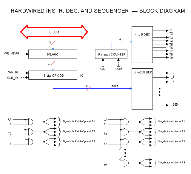
|
The whole purpose of this circuit is to obtain the exact control signals that we need for each clock cycle (T) for each instruction (i). In this view, Op Code Fetch (i_0) is just a particular case.
Note that the instruction byte is not read directly from the bus into the IR register but in the MDAR register instead. This is because we need the OP COD to be available along the entire life of the instruction cycle; we would lose it otherwise when reading an operand from the bus. When reading operands, they are read into MDAR while IR keeps the op cod for the rest of the instruction cycle. Signals WR_MDAR (latch into MDAR from the bus) and WR_IR (latch into IR from MDAR) are not simultaneous but separated in time by half a clock period.
We obtain signals T1 ... T9 (instruction "age") from the main clock, as illustrated. Separately we obtain signals i_0, i_1 ... i_255 (instruction being processed) from the op code.
For each instruction implemented in the CPU there is a simple logic similar to the one shown. It just combines each i_n signal with each Tm signal to provide the control signals needed for instruction, for time. In particular, there is a logic for i_0 (lower left corner in the diagram) which produces the sequence for the Op Code Fetch Cycle.
Signals internal to the IDS such as WR_MDAR, WR_IR, CLR_IR etc. are generated too from these little logic blocks. In particular each instruction must end its sequence by clearing the counter (T_CLR) which forces the appearance of T1, and clearing the IR register (CLR_IR) which forces the next Fetch Cycle.
Schematics
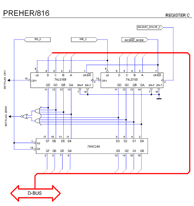
 Register C Register C
06/13/2009
This is a first attempt to implement registers that can be incremented or decremented without ALU operation so INC/DEC intructions execute in one clock cycle (Signal INC/DEC_PULSE_C).
|