Central Processing UnitThis section describes the Central Processing Unit (CPU) in great detail with the purpose of allowing the Engineer to fully understand how it works. Partial schematics are given. For complete schematics refer to section 'Schemtatics' at the end of this Manual.
Construction
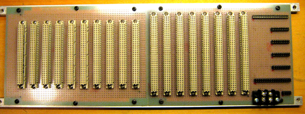
The Central Processing Unit (CPU) is housed into a rack mount frame containing a Backplane (back) to which several boards attach and a Console Assembly (front) composed by panel-mount buttons and switches plus four "floating" boards that provide Lamps buffering, Switch debouncing and Console functionality.
All CPU interconnections are made throughout the Backplane. Absolutely no cable is attached to any of the CPU boards that plug to the Backplane.
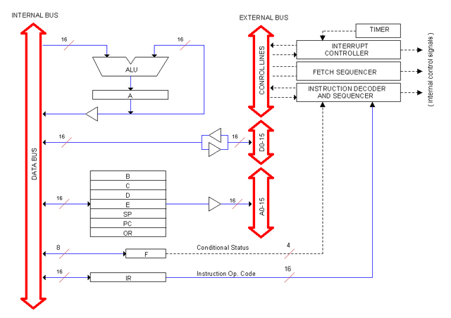
Block Diagram
CPU registers are grouped (for better understanding) into these categories:
- General Purpose (B, C, D, E)
- Special Purpose (A, PC, SP)
- Hidden (IR, OR, F)
- Console (LAR, LDR, SW)
All of them are 16-bits except F, the Flags register, which is 6-bits.
Registers communicate each others throughout two internal buses: Data Bus (D-BUS) and Address Bus (A-BUS, which is not shown in the diagram for simplicity). General purpose registers can read from the D-BUS and write to both. Special registers PC (program counter), SP (stack pointer) as well as the hidden register OR (operand register) can also read from the D-BUS and write to both.
The purpose of this arrangement is to allow indirect addressing from any of the general purpose registers. For example, an instruction making use of E as a pointer to memory will make it to write its content to the A-BUS.
The operand register (OR) is the destination for the operand during an Operand Fetch Cycle. For immediate addressing instructions, the operand is an immediate value; during the Execution Cycle, OR will write to the D-BUS. For direct addressing instructions, the operand is an address; during the Execution Cycle, OR will write to the A-BUS.
The External Bus consists of 16 lines for Address, 16 for Data and 7 lines for Control. It connects with internal buses throughout 3-state buffers as shown.
Register A is the "accumulator". The block diagram shows A in mutual relationship with the ALU. In fact, the accumulator is the only destination for ALU operations; it can also be used as a general purpose register with the only limitation that it can not write to the A-BUS so it cannot be used as a pointer to memory.
The Flags Register (F) contains four conditional status flags: Zero (Z), Negative (N), Carry (C) and Overflow (V). Two Additional bits hold the status of Interrupt Enabled (IE) and Timer Enabled (TE) conditions.
All Flags are set or reset using dedicated lines not shown in the diagram. Additionally, the Flags register connects to the D-BUS so it can be saved and restored to/from the Stack during CALL instructions or Interrupts.
Console registers (LDR, LAR and SW, not shown in the Blog Diagram) are managed by the Console Controller. SW is actually a 3-state buffer to the D-BUS. LAR and LDR output directly to the ADDRESS and DATA Lamps displays (respectively) located in the Console's front.
All CPU internal control signals (except those for Console registers) are generated in a circuit called Instruction Decoder and Sequencer (IDS, actually built with more than one card). The IR register output goes directly to this circuit to provide the current instruction code being decoded and executed.
Sequences for Op. Code Fetch and Operand Fetch cycles are generated by a separate circuit called "Fetch Sequencer". Interrupt sequences are built separately by the Interrupt Controller card.
Synchronization between controllers (Fetch Sequencer, IDS cards and Interrupt Controller) is assured by Status signals S0,S1 and Sequence Encoded Time ET0, ET1 generated by a Master Controller card. This card also contains the Flags register (F), the Master Clock generator and some other important circuits.
A Timer circuit interrupts the CPU at regular intervals for providing the "computer's tic". This can be enable or disable both from software and from the computer's Console.
Internal Buses
CPU internal buses are all wired in the Backplane. Those are the following:
-----------------------------------------------------------------------
Name Lines Descript
-----------------------------------------------------------------------
A-BUS 16 Address bus
D-BUS 16 Data bus
L-BUS 16 Lamps bus
S-BUS 4 Conditional Status source feding the flags register (F)
CS-BUS 4 Conditional Status: F unbuffered output to IDS cards
IR 16 Instructions Register unbuffered output to IDS cards
RST 1 Master Reset signal
CLK 1 Master clock (4MHz)
ET0,ET1 2 Sequence Encoded Time (T1,T2,T3,T4)
S0,S1 2 Machine Operational Status (Halt, Fetch, Exec, Interrupt)
C-BUS 80 Control Bus: All internal control signals wired as a bus
for all IDS card slots (12-18)
-----------------------------------------------------------------------
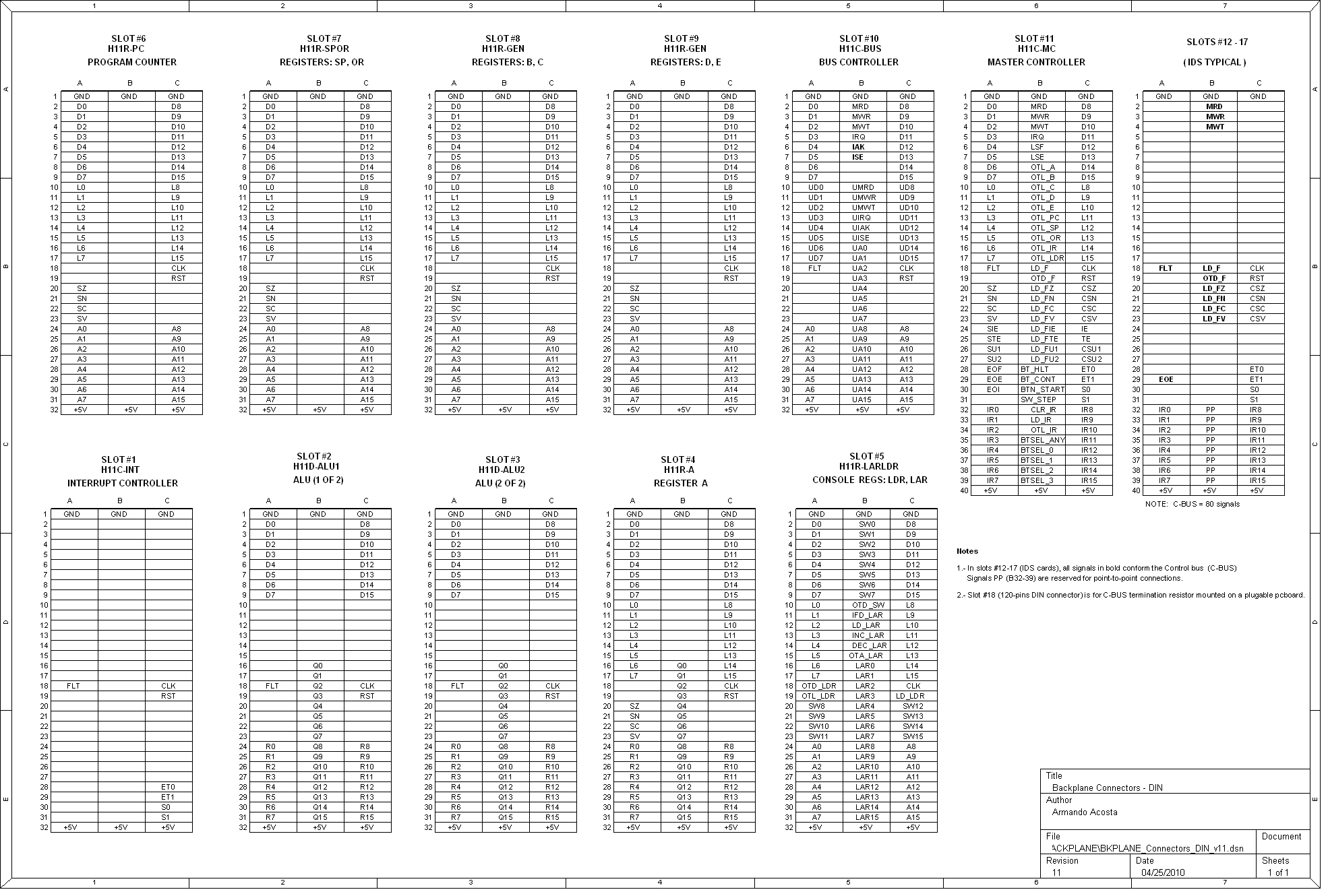
Backplane
The Backplane consists of ten 96-pins and eight 120-pins DIN 41612 female connectors, seven header connectors and one 2-POS terminal block connector. This later is for power supply (5V).
Each DIN connector occupies a "Slot"; these are enumerated from left to right: Slot#1... Slot#18. The terminal block connector is termed JP1. Headers are enumerated from bottom to top: JP2... JP8.
All connectors are wired in the back to compose the various internal buses of the CPU. Some Point-To-Point connections between different Slots also exists. Termination resitors for internal buses are placed (soldered) in the backplane.
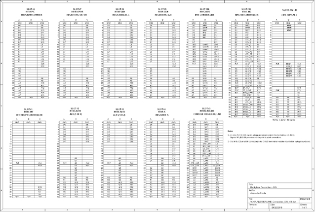
CPU Boards
-------------------------------------------------------------
Board Name Description Location
-------------------------------------------------------------
H11C-INT Interrupt Controller Backplane Slot #1
H11C-BUS Bus Controller Backplane Slot #2
H11D-ALU1 ALU board 1 Backplane Slot #3
H11D-ALU2 ALU board 2 Backplane Slot #4
H11R-A Register A Backplane Slot #5
H11R-LARLDR Console registers (LAR, LDR) Backplane Slot #6
H11R-PC Register PC Backplane Slot #7
H11R-SPOR Registers SP, OR Backplane Slot #8
H11R-GEN Registers B, C Backplane Slot #9
H11R-GEN Register D, E Backplane Slot #10
H11C-MC Master Controller Backplane Slot #11
H11C-IDS1 IDS card 1 Backplane Slot #12
H11C-IDS2 IDS card 2 Backplane Slot #13
[ More IDS cards may exist on slots #14-18 ]
H11D-CONL Console Lamps (left) Console assembly
H11D-CONL Console Lamps (right) Console assembly
H11D-CONB Console Buttons (+Stu Lamps) Console assembly
H11C-CONC Console Controller Console assembly
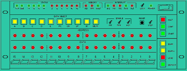
Console Assembly
[...pending]
|