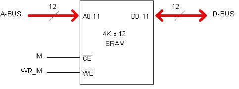
Memory implementationHER/12 memory is part of the CPU equipment and it is not extensible.
It is implemented using three SRAM chips, 4K by 4 bits each. Since the chips are directly addressable using the 12 bits available in the A-BUS, no decoding logic is needed: chips address pins are connected together and directly to the A-BUS. Same can be said about chips control pins CE (Chip Enable) and WE (Write Enable). Data pins are distributed among the 12 lines of the D-BUS.
The memory chips employed are very fast (35 ns). A half-clock period (42 ns) is long enough to have an stable data in the bus once the address and OE signals have been applied. Consequently, no synchronization logic is needed being the memory as fast as the CPU circuitry itself.
Control signals related to Memory are the following:
* M Connected to chips OE pins. Asserted for either reading or writing in Memory.
* WR_M Connected to chips WE pins. Asserted for writing in Memory.
Memory Read Cylcle
The Memory Read Cycle takes one clock period.
Fist, the M signal is asserted. Also the address is put in the A-BUS at this time. As a result, the content of the addressed memory cell appears in the D-BUS.
Half clock cycle later (42 ns), this data is sufficiently stabilized in the bus. With the falling edge of the clock (in the middle of the cycle), the appropriated control signal WR_r is asserted to latch the data into the target register r.
At the end of the clock period, all signals are released.
Memory Write Cycle
The Memory Write Cycle takes one clock period.
All necessary signals are put in the buses at the begining of the clock period. These signals are: Address in the A-BUS, data in the D-BUS, M and M_WR.
Half clock later (42 ns), signals M and M_WR are pulled up. This makes effective the write operation into the memory chips.
At the end of the clock period, all signals are released.
|