SynchronizationSequences of control signals are generated by four "sequencer" circuits. Those are:
* Fetch Sequencer
* Exec Sequencer
* Interrupts Sequencer
* Console Sequencer
These circuits are purely combinational, taking inputs from various "status signals" generated by a "Master Controller" circuit, and producing the different control signals at the outputs. The Instruction Sequencer in particular also takes input from register IR to produce sequences pertinent to the current opcode, effectively decoding the instruction.
All control signals are active low.
Master Controller
The Master Controller circuit contains the following elements:
* Master Clock Oscillator
* Encoded Time generator
* Arbiter
Master Clock oscilator
The master clock (12 MHz) is generated by this circuit. This clock is the time-base for producing all other master and control signals, which in turn are the time-base for producing sequences of control signals.
Encoded Time signals (ET0, ET1, ET2)
Encoded Time signals ET0, ET1, ET2 represent an ascendant count (named "ET count") generated by a counter circuit clocked by the Master Clock. The count rolls over from 111 back to 000 if not terminated (reset) earlier.
Counts are conventionally named T1, T2,..., T8 as shown below:
ET0 ET1 ET2 Name
--------------------------------------
0 0 0 T1
0 0 1 T2
0 1 0 T3
0 1 1 T4
1 0 0 T5
1 0 1 T6
1 1 0 T7
1 1 1 T8
--------------------------------------
These signals are inputs for the different sequencer circuits and serve to define sequence steps. Most sequences are short, taking only one or two steps. The longest are related to interrupts and CALL instructions and take eight steps to complete.
Arbiter and Master Status signals (S0, S1)
The machine is always in one and only one of the following states:
* Halt
* Interrupt
* Fetch
* Exec.
The Arbiter circuit dictates the computer's state by the mean of two master status signals (S0, S1), utilized to select the appropriate Sequencer, as shown in the table below. Only one sequencer is active at a given time.
-------------------------------------------------------------------------------------------------
S0 S1 State Active Sequencer Descript
-------------------------------------------------------------------------------------------------
0 0 Halt Console Sequencer Halted
0 1 Interrupt Interrupt Sequencer Taking care of interrupt before calling the ISR
1 0 Fetch Fetch Sequencer Instruction Fetch cycle
1 1 Exec Exec Sequencer Instruction Exec cycle
-------------------------------------------------------------------------------------------------
In terms of implementation, S0 and S1 are distributed in a bus (C-BUS, for "Control Bus") along with other signals to reach the different sequencers. Each sequencer is wired to inhibit itself unless S0,S1 have the appropriate value. Also wired in that bus is a signal named EOS (End Of Sequence), imputing the Arbiter. Sequencers pull this signal down when the sequence they produced comes to an end.
The Arbiter circuit generates the master status signals S0, S1 according to the following logic.
After reset, S1,S0 = 0,0 (Halt), and remains in that state until the button RUN is pressed in the Console.
Pressing the button RUN causes the Arbiter to reset the ET count and set S1,S0 = 1,0 (Fetch). Consequently, the next clock period becomes the time T1 for the Fetch Sequencer which generates a Fetch sequence. With the falling edge of the clock in the middle of the last cycle, signal EOS is pulled down by the Fetch Sequencer to notify it has finished.
In reaction to the EOS signal, the Arbiter resets the ET count and puts S1,S0 = 1,1 (Exec). Consequently, the next clock period becomes the time T1 for the Exec Sequencer, which starts the corresponding sequence.
The exec cycle can take from 1 to 8 clock periods depending of the instruction. When finished, the Arbiter is notified via EOS signal.
In response, the Arbiter resets the ET count and checks if there is an Interrupt request. If that is the case and interrupts are enabled, the Arbiter puts S1,S0 = 0,1 (Interrupt), otherwise S1,S0 = 1,0 (Fetch).
In case of interrupt, the Interrupt Sequencer generates a sequence to push registers PC, F, S to the stack, then to load PC with the ISR address. After that, the Interrupt Sequencer sends the EOS signal in response to which the Arbiter resets the ET count and put S1,S0 = 0,1 (Fetch) effectively starting the ISR routine.
Notice that the Fetch, Exec and Interrupt sequencers run one sequence at the time and then return control to the Arbiter. The case of the Console sequencer is different in this respect, since it can run an undefined number of sequences at the Operator's request without returning to the Arbiter. This is a potential problem which solution is this: the Console Sequencer does not take ET0, ET1, ET0 signals as inputs; it generate the different sequence steps using internal timing. It follows that the Console Sequencer is not a pure combinational circuit as other sequencers are.
Instruction Fetch Cycle
The Instruction Fetch Cycle is generated by the Fetch Sequencer when status signals S1,S0 equals: 1,0.
The sequence takes one clock period, being a memory read cycle (as explained earlier) using register PC as the address provider and IR as the destination register.
The Program Counter register (PC) is incremented during T1 of the Exec cycle overlapping this operation with others pertinent to the current instruction's Exec cycle.
Instruction Exec Cycle
The Instruction Exec Cycle is generated by the Exec Sequencer when status signals S1,S0 = 11.
The Instruction Sequencer has IR for input, so sequences are assembled depending of the current OpCode, effectively decoding and executing the current instruction.
We will not cover all instruction sequences in here; suffice is to say that they can vary taking between 1 and 8 clock periods to complete, depending of the instruction.
The first period (T1) is always used to increment the Program Counter (PC), in addition to produce the control signals pertinent to the instruction per se. To do this, signal INC_PC is activated at the beginning of T1 and will remain activate all T1 long; consequently, PC will be effectively incremented with the falling edge of the clock in the middle of T1. This must not cause any problem as long as the instruction in course is not working with PC. If it is (for example, a branch instruction) then WR_PC will compete with INC_PC at half T1. The dispute is resolved in favor of WR_PC thanks to proper design of the PC register circuitry.
The case of instructions with Immediate Addressing is special because the operand is in the memory word pointed by an incremented PC. In this case, period T1 is dedicated to just increment PC; control signals to perform the actual transfer will appear at T2. The next period (T3) is used to increment PC further so it points to the next instruction in memory.
Notice that the instruction LDI PC value will result in PC=value+1, because, as mentioned, PC is incremented at T3 of the exec cycle.
When the Instruction Exec sequence finishes, all signals are released and signal EOS to the Arbiter which, in response, will set to put S1,S0 = 1,1 so a new Fetch cycle can start at the next clock period.
Example of a sequence built with combinational logic
To illustrate how sequences are built in HER/12 sequencer circuits, we will consider the execution of a simple instruction:
LDR A, B
which causes the content of register B to be copied into register A.
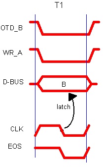
The instruction's exec cycle completes in one clock period (T1), as illustrated in the time diagram below.
First, both OTD_B, WR_A control signals appear simultaneously, causing the content of B to be put in the D_BUS. Register A, however, won't latch until the next falling edge of the clock. This is due to register's design as we discussed previously. With that falling edge we also fire the End Of Sequence signal (EOS).
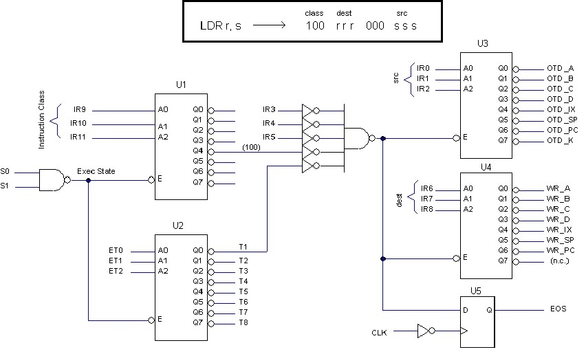
The instruction is encoded in a generic way valid for all registers, as discussed in section "Instruction Set Architecture (ISA)". If bits 11,10,9 (instruction class) are "100" and bits 5,4,3 are "000", then the following circuit will generate the intended sequence; otherwise, none of the output control signals will be activated.
Fist of all, S0,S1 must be "11". Notice in the diagram that all decoders will be inhibited otherwise causing all control signals at the output to be 1 (inactive).
Secondly, the "instruction class" must be "100"; otherwise decoders U3, U4 will be inhibited producing no signal at the output (all ones).
Third, the control signals appear at T1, that is, when E0,E1,E2 = "000".
Finally, bits 5,4,3 must be "000", and this is specific to this instruction in particular.
Decoders U3, U4 decode the appropriate source and target registers directly from the instruction's code. In this case, OTD_B and WR_A would be produced.
The "End of Sequence" (EOS) signal is generated synchronous with the clock by U5..
In fact, this circuit is part of a bigger one. Other sequencer circuits similar to this would be connected to the others U1's outputs, one for each instruction class. Those circuits would take signals T1, T2,... etc, from U2, as appropriate.
This circuit is only an example. Possibly it deserves better design, but it illustrates the following general rules:
* Instruction sequencer circuits inhibit them self is S1,S0 is different from "11" (exec state).
* Different instruction classes select different sequencer circuits.
* The ET count (E0,E1,E2) define different steps within the sequence.
* Fields encoded in the instruction (such as registers) are decoded directly by sequencer's circuitry.
|