Breadboard testingDuring this phase I will be doing design and testing, one part at the time, in the form of separate experimental circuits.
Fetch Sequencer
08/11/2009
Today I finished building this little experimental circuit and started to test. The experiment revealed some design problems but it started to work as expected after minor changes were made.
This is the first test of a "sequencer". The technique tested here will also be used for decoding instructions in IDS cards. Here is the schematic for the working test circuit:
Introducing the L-BUS
8/20/2009
Today I introduced a new CPU internal bus named: L-BUS (Lamps Bus). This 24 lines bus will be present in Data Slots specially for registers.
Registers will write to the L-BUS so its content can be displayed in dedicated LEDs on the Console. At a given time only the selected register writes to the bus (selection comes from the Console). The first 16 lines (L0-15) are for register's content whereas L16-21 show the current status of the register's control signals: CLR, LD, INC, DEC, OTD, OTA. Lines L22 and L23 are wired but not used and always read "inactive" (wired to +5V since all control signals are active low).
Now registers feature a third output buffer (in addition to the two they already had) and a new input control signal named: OTL (Output to Lamps) which selects the register to be shown.
This simple idea have brought three consequences to me:
1.- Registers are now bigger (and more expensive), not very easy to fit more than three of them in a card of 5.5x8 inches.
2.- I can not longer draw for letter-size sheets but for 11x17 inches instead.
3.- The way for the Console's operator to read register's content is now a lot easier.
To be honest I had opposed to this idea until now. That is because I wanted to restrict the Operation to the CPU architecture, that is: if one wanted to see a register content, then he or she needed to open that register to the internal D-BUS (switch OTD, Open to Data Bus).
However, when I started designing the Console's control circuitry, I found that the interconnection between this card and the Master Controller Card were taking too many pins. I found other problems related to selection logic so I decided to "distribute" the selection among register cards, hence the L-BUS.
The Operator (... what operator apart from my self?) will be happy with the new design since now he will be able to watch any register content (as well as their control signals) very easily by just selecting it... not sure if by mean of push buttons or a rotary key.
Introducing the Arbiter Circuit
08/23/2009
Until now, control coordination between the Fetch Sequencer, the IDS cards and the Interrupt Controller relied on four "status signals" (SH, SF, SE, SI: Status Halt, Fetch, Execute and Interrupt respectively).
Problems arose when I started to sketch the actual circuits. These signals came from different places to fight each others under inhibit/enable rules. At the implementation level, that proven to be a mess.
I came today with a different, much more decent approach. Now the status is coded in two signals named: S0 and S1, according with the following table:
S1 S0 Status
- - - - - - - - - - - - - - - - - - - - - -
0 0 Halt
0 1 Fetch (either code or operand)
1 0 Execute
1 1 Interrupt being negotiated
These signals comes from a new circuit called ARBITRER. IDS cards and the Interrupt Controller listen to them and keep themselves inhibited until the appropriate status arrives.
When execution finishes, the IDS generate an "End Of Execution" (EOE) signal back to the ARBITER which in turn generates the appropriate signals to either halt the computer (case of STEP execution) or clear the IR to enforce the new Fetch cycle. Similarly, the Interrupt Controller rises an "End of Interrupt" (EOI) when negotiation with peripheral is over.
Small Cards: a challenge
08/26/2009
The challenge that using small prototyping cards represents is becoming more and more apparent.
For one part, register circuits have grown during the last week. Recently, the L-BUS was introduced and now I'm wondering how I'm going to raise flags and even detect fault conditions from the registers themselves. That will be by adding more chips, obviously. Will them fit?
In the other hand is the connector pin-count issue. I have designated 70 of the 96 pin available at Data Slots so only 26 are left for point-to-point control signals. My "standard signals" add 6 per register so the pin-count by itself limits my cards to have 4 registers at the most with only 2 pins left for additional signals.
That still matches my original plan (PC, SP, OR in one card; B, C, D, E in another card and A in the ALU card) but feeling as being pushed to the limits is not nice.
As per Control Slots (120 pins), 37 pins are designated already, 83 are available. A comprehensive count of register's control signals resulted in 55 total so there are still 28 pins available.
Not all of these remaining 28 pins can be connected in a bus (as the others are) because I will need a few of them (about 8) for point-to-point connections. For instance, the "End Of Interrupt" (EOI) signal coming from the Interrupt Controller.
I wouldn't like to make more significant changes to the design so for now I will keep going on with this tight situation.
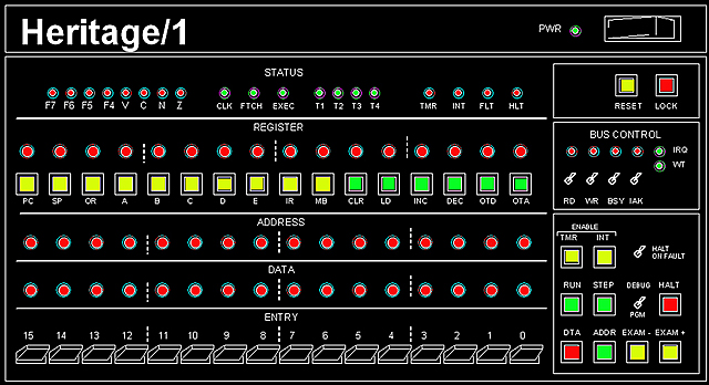
Control Panel Layout
8/28/2009
I'm kind of stocked with the Arbitrator and the commands comming from the Control Panel, but I hope to solve that soon. The Control Panel (or Console, as I also call it some times), is almost definetely decided. It will look more at less like this:
The illuminated square buttons cost about $15 each so not sure if I will use exactly those.
Memory Bank register: defeated!
A few days ago, I submitted the project to comprehensive revision under severe criticism. I wanted to make sure that all the ideas developed so far were strong enough. Most of them hold; some (such the Interrupt Architecture) resisted not without difficulties. The only one that did not pass was the use of Memory Banks (register MB).
This technique seeks two purposes: (1) To expand the "limited" 64K words memory address space, and (2) to provide a rudimentary hardware support for General Protection in the future. Neither of these arguments proved strong enough; here is why.
The 64K words limit
From the "historical" point of view, 64K words matches the old-fashioned technology being employed. Most minis in the 60s and 70s came equipped with about 8K words, being 64K a costly luxury. It was using one of those minis (DEC DPD-11) that the UNIX operating system was invented.
From a realistic viewpoint, I'll be writing software in plain Assembly language for a long time. Even when I could envision the developing (or porting) of a full featured operating system in the far future, it is hard to imagine the need for more that 64K words of memory due the kind of software that Heritage/1 will be able to run in practice.
Lets imagine, however, that 64K proved limited at some point in the future. In that case, I will be happy then to accept the challenge to start developing solutions both in software and hardware.
Rudimentary support for General Protection
Years will pass before I embark into Protected OS development and chances are for so to never happen at all. Hence the weakness of providing such a support from the very beginning. Besides, I cannot tell if memory banks (allocating different processes in different banks) will actually work.
Conclusion
The removing of the MB from the architecture honors the original idea of having data and address the same size. Software will get simplified by not having to declare the current memory bank. Circuitry will also gain in simplicity.
As per the subjective side of the project, I now feel better to have a decent provision of memory that matches the historicity of the machine being built.
The only thing that is still bodering me is the use of modern SRAM memory chips. That, however, will be very hard to "fix".
Introducing Relative Branches
09/22/2009
Last night I was thinking on how an Operating System (even the most rudimentary one) would manage to allocate programs in memory from Storage. I realized that those programs must be written using relative addresses instead of fixed ones. That could be done using the already provided "indirect branch" instructions (such as "JNZX reg"), but the correct way is to implement actual "relative branch" instructions.
For implementing this new addressing mode, some modifications need to be made. Fortunate the modification in question is quite simple and, after all, the computer is still on paper (nothing has been built yet) so this is the time.
The new addressing mode (relative) will only apply to branches because extending the concept to all registers would lead to profound changes to the overall architecture. I don't want that.
An example of relative branch instruction is this:
jnzr OFF_SET
where OFF_SET is an operand to be fetched from memory (following the op code). Executing this instruction will cause the Program Counter to add OFF_SET to its current content so the next op code fetch takes place OFF_SET memory locations further.
This will allow an OS to allocate programs anywhere in memory since those programs won't care about where they are but only how far they need to jump.
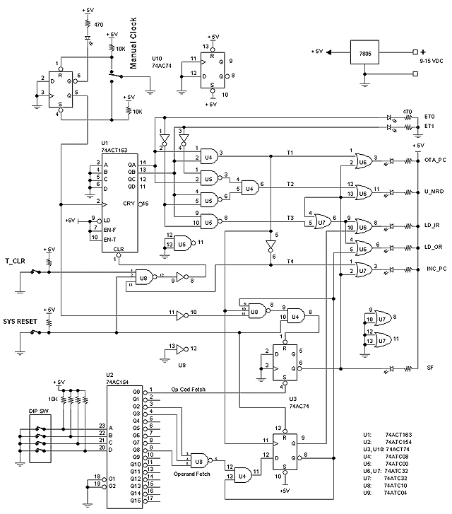
Arbiter circuit tested
10/3/2009
Today I tested this simple Arbiter circuit, which proved correct.
The circuit was built in a prototyping board and tested using simulated signals coming from debounced switches. Output signals S0, S1 was displayed using buffered LEDs.
Principle of Operation
The circuit is actually a Finite State Machine (FSM) implemented with two D-type flip-flops (74ATC74) which outputs represent the status signals S0, S1. A simple combinational logic takes those, combined with others, and feeds the data (D) flip-flop's inputs with the "next status". The FSM changes status when the flip-flops are clocked by a "stimulus" signal provided by a logical OR of all possible "stimulus signals": /EOF, /EOE, /EOI, /START. (Note: In the diagram, the "logical OR" is actually a logical AND (U1) because input signals are active low).
The /START signal is a "pulse" provided by the Control Panel circuit. It occurs when the Operator pressed either HALT, RUN or STEP button on the Console.
The status output signals S0, S1 represent the current status of the computer, according to the following table.
S1 S0 Status
- - - - - - - - - - - - - - - - - - - - - - - - - -
0 0 Halt
0 1 Fetch Cycle
1 0 Execute Cycle
1 1 Interrupt being negotiated with peripheral
- - - - - - - - - - - - - - - - - - - - - - - - - -
Different circuits (such as the Fetch Sequencer, the IDS cards and the Interrupt Controller) use those as enable/disable signals. For instance, the Fetch Sequencer inhibit itself when S1,S0 is different from 0,1.
After reset, the Arbiter is in Halt status (S1,S0 = 00). When the operator pushes the RUN button on the Control Panel, the Halt flip-flop gets reset (/HLT=1) and the Arbiter changes status to S1,S0 = 01 to allow the Fetch Sequencer to start a new Fetch cycle.
Once the Fetch is completed, the Fetch Sequencer rises an "End of Fetch" (/EOF) signal which forces the Arbiter to change status to S1,S0 = 10; this authorizes IDS cards to start the Exec cycle.
When the Exec cycle finishes, the IDS card rises an "End of Execute" (/EOE) signal, signaling the Arbiter to change status again. The Arbiter decides what next according to the following logic:
If the Halt flip-flop is reset (/HTL=1) and there is not a pending interrupt request (/IRQ) from the Interrupt Controller, then:
- - - - - - - - - - - - - - - - -
Current --> Next
- - - - - - - - - - - - - - - - -
0 0 --> 0 1 Go Fetch
0 1 --> 1 0 Go Exec
1 0 --> 0 1 Go Fetch
1 1 --> 0 1 Go Fetch
- - - - - - - - - - - - - - - - -
If the Halt flip-flop is set (/HLT=0), the output is forced to S1,S0 = 00.
If there is a pending IRQ, the output is forced to S1,S0 = 11 which authorizes the Interrupt Controller to start the Interrupt Sequence (negotiation with the interrupted device). When the sequence finishes, the Interrupt Controller drops the /IRQ signal and rises an "End of Interrupt" (/EOI) signal; in response, the Arbiter change status to 01 (Fetch).
Neither /IRQ nor /HLT signals will be sensed until the last execute cycle has finished, that is, when /EOE is active. This ensures that no instruction cycle will be left behind in the middle of the battle.
|