The Heritage/1 LAB implementationDuring this phase, a LAB implementation of Heritage/1 will be built. The final machine will be built much later, after the "LAB" has became mature and fully functional. Most parts from the LAB will be reused to build the final machine.
Wiring the Backplane
10/10/2009
I started to wire the backplane consisting of 6 "Data Slots" (96 pins), 6 "Control Slots" (120 pins) and one "interconnection slot". I've seen that this is quite a slow task since it took me 10 minutes to wire just one of the numerous bus lines. Nevertheless I plan to have the Backplane wired by 10/24/2009.
What about "micro-dioded" logic?
10/12/2009
Considering the use of small diodes matrixes. See discussion in the BrainStorm book:
http://www.armandoacosta.com/cpu/index.php?branch=390
Entry Swithes: just another register
10/19/2009
Here is a simple idea, so simple that I still wonder why it didn't occur to me before: The Entry Switches are nothing but another register within the CPU.
For "normal" registers, I have a set of lamps and buttons on the Console to select one register at the time, show its content as well as it's control signals status and also to CLEAR, LOAD, INC, DEC and open its buffers to either the internal Data Bus or the Address Bus. Well, if Entry Switches are another register, then it must be present in that buttons/lamps set.
Thus, I will simply add another button labeled "SW"... (in place of the "MB" wich is not longer needed).
By pressing that button, the operator selects the Entry Switches for watching its content in the lamps. He also will be able to dump its content to the Data Bus (button "OTD") or to the Address Bus (OTA) as with any other register.
For example, if I want to load the IR register from the Entry Switches, I press the "SW" button, enter the desired content in the switches, then I press the "OTD" button so the content is available to the internal Data Bus; then I select the IR register by pressing the "IR" button and then press the "LD" button to load that register from the Data Bus.
That is when the computer is in "Debug Mode". In "Programming Mode", the Entry Switches behavior will be totally different. In Programming Mode, the operator needs to be able to examine and/or alter memory content and to run a program starting in a given (by switches) memory address. But that is an old story, I mean, I had conceived that part before.
Two boards for one Console
10/26/2009
I haven't find a clean, elegant solution to the problem I had with the Console, until now (a few minutes ago). The problem is this:
The Console is a "controller", actually the "ultimate resource" when things go wrong with the computer circuitry. But the Console is not just a bunch of lamps and switches but logic as well so it takes board space (more than I expected) and, what is worse, it takes a lot of pins.
I were conceiving a "Console Board" to allocate such logic, but this board would not attach to the Backplane but to the "Master Controller Card" which in turn plugs to two slots (Data and Control) being the only card in the CPU with such a privilege. The Console needs signals from both Data and Control slots hence the need for been connected to the Master Controller Card.
This arrangement never pleased me but no better idea had came to my mind. The worst part is the large amount of interconnections between the Master Controller and the "Console Board", made with ribbon cables plugged to header connectors (something that I truly heat!)... By the way, all this is still on paper, nothing has been built yet.
And, yes, fortune smiled to me just a few minutes ago when I came with a different approach which is this: No one but two Console boards.
One is called the "Console Monitor Board" and it plugs to a Data Slot just as Registers cards do. This cards is responsible for collecting and buffering data from the buses (D-BUS, A-BUS and "Lamps Bus") just to be presented on the Console's lamps (LEDs). It also contains the Entry Switches Register.
The other card is called the "Console Controller Board" and plugs to a Control Slot just as other controllers (such as IDS and the Interrupt Controller) do. It contains the Console's logic and rises internal control signals in the same fashion other controllers do.
So there is nothing special with "console boards"; they are regular "data" and "controller" cards and they follow exactly the same rules. This solution will simplify wiring and will allows me to allocated the different Console's circuits in a comfortable manner.
I think this solution is elegant, but what makes me really happy is to see how the overal design is guiding my mind to every specific solution in a natural way, so it makes me to conclude that the design is, indeed, an elegant one.
Removing sixteen LEDs from the Console!
10/31/2009
While sketching the Entry Switches registers, I realized that I don't really need dedicated LEDs for monitoring the internal DATA BUS. In fact, the L-BUS allows the operator to select whatever he wants to watch so I can simply let him select the DATA BUS as well, in the same way he selects any other register.
What I had named "REGISTER" (LEDs) now becomes the "DATA" LEDs. And what I'd named "DATA" (LEDs), simply disappear.
As per Entry Switches, I don't need to latch them during Debug Mode. The operator can treat the Entry Switches as any other register only that a manual change in the switches themselves will be reflected immediately.
For Programming Mode, I will introduce two specialized registers called "Programming Data Register" (PDR) and "Programming Address Register" (PAR). These registers will be used by sequencer circuitry located at the Console Controller Card for performing the memory data read/write cycles required during Programming Mode.
|
This new arrangement not only simplifies wiring (16 less connections!) but it also fits better within the overall design.
Three registers will not fit in a single card
11/04/2009
Registers have gone too big, specially with the addition of logic for detecting Conditional Status. A typical register such as B, takes 14 chips plus additional logic so the three registers per card that I've planned would take more than 42 chips which definitely don't fit in a 8x5.5 inches prototyping card.
I have two options: (1) To use larger prototyping boards, (2) to distribute registers in a different way (2 regs per board at the most). The former is too expensive; the right card costs almost twice (about $20.00 from Digi-Key) that my 8x5.5 inches boards. Hence I'll take the second choice.
Here is the new distribution:
Card Name Registers
- - - - - - - - - - - - - - - - - - -
H1-REG1-1 PC, OR
H1-REG2-1 SP
H1-REG3-1 B, C
H1-REG4-1 D, E
H1-ALU-1 A (and the ALU)
Concern with the idea of having a "Control Bus"
11/10/2009
For more than four months the design has kept stable based on certain "primary ideas" that have hold so far. One of those ideas is to wire all control signals together in a bus in "Control Slots" so all Controllers have access to those at the same time. This allows me to have more than one IDS (Instruction Decoder and Sequencer) card, which is good because it represents modularity which is convenient.
There is a price to pay, however: the increase of pin-count. I was been forced to purchase expensive 120-pins connectors for "Control Slots" just because of that. And not just money; another problem is with the Console, which takes many interconnections, that is many ribbon cables plugging to header connectors anywhere within the computer, which is a mess.
That's why I am revising the "primary idea" of the "Control Bus" in the sake of solutions. I wish to have all conations through the Backplane only: not a single ribbon cable plugged to any card at all. The only way I could get to that is by removing pin assignments from the Backplane connectors. The obvious opportunity is with the Control Bus.
I realized that the only cards that really need access to all control signals are the IDS cards. Other controllers such as the Interrupt Controller and the Console Controller only deal with a few control signals. Therefore there is no need (other than simplicity) to wire all 75 control signals to all Control Slots; it is sufficient to wire them to IDS slots. This would free a lot of pins for the Console Controller that could be used to connect to the Console.
The bottom line is to defeat the simple idea of having just two types of Slots (Data and Control). The new approach would be to wire the Backplane more efficiently putting wires where is really needed.
Honestly, I'm not entirely happy with this approach because it will prevent the mess of ribbon cables at the expense of creating a mess in the Backplane wiring. So I'm not making a final decision yet, but just researching the matter very carefully.
The fall of two milestones
11/21/2009
Last week was busy in terms of crucial decision making. If Heritage/1 were a real machine being designed by a real-world manufacturer, last week were be one of hot meetings and heavy memos.
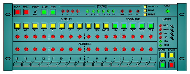
Two milestones was definitely defeated: The division of the Backplane in DATA and CONTROL slot types, and the old idea that the Console must offer static hardware debug capabilities.
The former opens an important opportunity: the possibility of wiring the Console's panels directly to the Backplane via ribbon cables ended with header connectors. So far I simply had no pins left in the Backplane connectors for that so ribbon cables had to connect to a card which is not a clean solution.
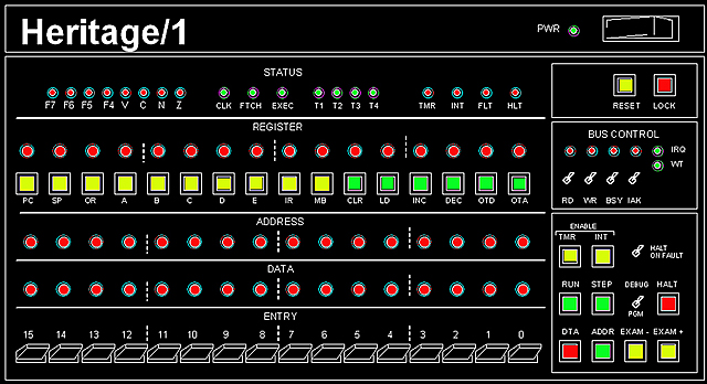
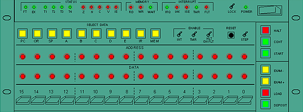
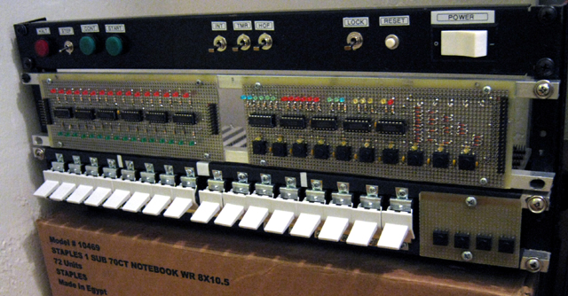
The later resolves a tremendous bottleneck that I had with the Console's design since "debug capabilities" turned very complex in implementation. Its removal has lead to accelerate the project in a notable manner. Here is the new Console without hardware debug capabilites:
The Ruch for the Backplane
12/01/2009
I'm moving to produce a Backplane as quick as possible. Having the Backplane and the Console (not only the actual panels but also the boards that provide its functionality) I will be able to move the project into �scalade mode�, that is building the machine board after board.
That's why I am a real ruch to finalize designs for both the Backplane and the Console. They are actually, pretty much, finished so I'm making preparations for ordering the necessarry parts.
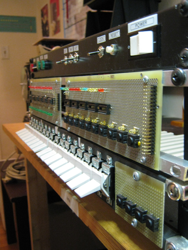
Console boards being built
01/26/2010
Panel circuits design is complete. It took four boards: two for push-buttons, LEDs and buffers, one for console registers and one for console functionality. The first board was built and the second well be finished soon.
Micro-dioded logic discarded
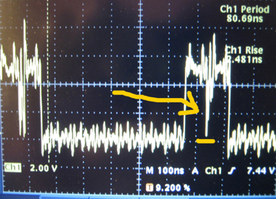
2/5/2010
I've been considering the use of diodes matrixes for a while, or what I called "micro-dioded logic". However, a simple "test of concept" experiment proved that the use of a diodes matrix for building sequences is not a good trend.
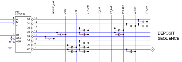
The images below shows a portion of the drawing. You can see the matrix rows being fed from the Decoder's outputs.
As expected (hence the purpose of the test), sparks appear at those points when the decoder's outputs change.
I could cut the spark with a simple RC low-pass filter circuit (R=100 Ohm, C=47pf), as shown bellow:
However, this is not the kind of solution I seek, so I decided to discard Diodes Matrix all together as a technique for building sequences.
Manuals
02/10/2010
Rearrenged the site to accomodate the Heritage/1 Manuals: Operator's Manual, Engineer's Manual and Programmer's Manual. The idea is to filter out old irrelevant content for having clear ordered up-to-date information into these books.
Two months of inactivity
04/09/2010
This project has been "frozen" for two months as I turned to other priorities that I have in life (including my work). Currently, my free time is still scarce but nevertheless I decided to retake the project in the aim of getting to the "escalade phase" as soon as possible.
I started by reviewing notes and schematics to proudly found that the project is in very good shape: implementation ideas and solutions are mature (stable) so I can continue by the exact point in which the project was left two months ago.
The focus now is into producing the Console and the CPU Backplane as those are the infrastructure required by the "escalade phase". The bad thing about it is that it will take long (about four months) and, because separate testing is not too feasible, all of those parts will possible be tested at once, hence to make them to really work will take even longer. I don't expect any thing truly functional before the end of this year.
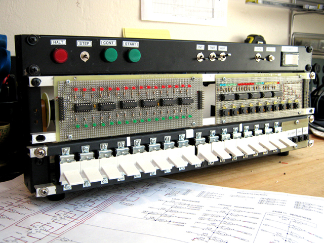
Building the Console Controller
05/05/2010
I'm currently building a board named: "Console Controller". It produces the sequences to carry out the Console commands: LOAD, DEPOSIT, EXAMINE- and EXAMINE+. It also handles other Console functions such as "Panel Lock".
This is important to the project as it will serve to prove two concepts: (1) The technique being employed for producing sequences by hardwired logic (see Building sequences with combinatorial logic) and (2) the construction technique being employed to actually wire boards by soldering (see Why are you soldering instead of wire-wrapping?).
So far, so good. The wiring process is quite slow but it is easy to make changes when needed. I do the wiring in two steps:
Step#1: I "prepare" the board by placing components and connectors, wiring power pins with naked wires and placing naked "half-moons" that will serve to guide signal wires is step 2.
Step#2: I patiently start connecting the signal wires using the "half-moons" as physical guides. Partial tests are performed during this step.
If I had a lot of time, building a board that way would take about a week. Unfortunately that is not the case so it is taking a little longer...
Writting the Heritage/1 Assembler
5/31/2010
Started to write an Assembler for Heritage/1, called H1ASM v.0.
I had no plans for start building my development tools yet. Moreover I was aimed to purchase a commercial cross assembler or to seek an open source one in the Internet. However, I started to think on how could I write one that is very simple. Soon I realized that it may be not too hard if I content my self with writing something really, really simple.
I started by cutting the Linker at once, that is my assembler will act as a "stand-alone" guy capable of directly generate the executable code. This leads to serious limitations indeed but it also simplifies tremendously the assembler on its own.
Macros were also discarted as well as conditional compilation and other "advanced" features that real assembler ususally offer. My assembler will be so simple that I'm not longer scared by the task of writing it entirely from scratch.
I chosen PHP command-line interface (cli) because it is easier than C, as code doesn't need to be compiled. Moreover, being PHP a popular scripting language, my assembler will be able to run on Linux, Windows or Mac OS-X and even ported for a web environment with little effort.
I started building the code up the point that I have a comfortable infrastructure. But now I'm more concern with the production of the Programmer's Manual, which is actually my SPEC for guiding my self during the development cycle.
The (unfinished) Manual is already published in this site, here is the link:
http://www.armandoacosta.com/cpu/index.php?branch=533
Reducing the Fetch cycle to 3 periods instead of 4
6/1/2010
Tonight, an old premise (held since July 2009) fall, resulting in a 25% increase of the average performance... according to raw calculations.
It was established since before that the Op. Code Fetch cycle should take 4 clock periods:
T1 Open PC to the A-BUS (OTA_PC)
T2 Memory Read signal (MRD)
T3 Read the bus into IR (LD_IR)
T4 Increment PC (INC_PC)
Since every instructions requires an Op. Code Fetch cycle, this T4 doing nothing else apart for incrementing the PC represented a serious waste of overall execution time. Here is how I took it away.
Following the Op. Code Fetch cycle is either the Operand Fetch cycle or the first period (T1) of the exec cycle.
I realized that PC is never used in execution during T1. Even branch instructions (the only ones that get to write into PC) don't touch that register until T2, so we are really plenty of time during T1 for activating the INC_PC signal in order to increment PC at that time. This will reduce the Op. Code Fetch cycle (as well as the Operand Fetch cycle) to 3 periods instead of 4.
So now we have:
---- Op. Code Fetch ---------------
T1 Open PC to the A-BUS (OTA_PC)
T2 Memory Read signal (MRD)
T3 Read the bus into IR (LD_IR)
--- Exec --------------------------
T1 Increment PC (INC_PC)... apart from whatever the instruction needs to do.
T2 ... the instruction continues to execute.
Doing the same for Operand Fetch cycle is also possible. PC was opened to the A-BUS during Op. Code Fetch and now it needs to remain open during Operand Fetch while it's being incremented (at T1); however the Memory Read signal (MRD) will not come until T2 (250 ns later) which is long enough for the data to stabilize in the bus... (I hope).
An additional advantage is that now the INC_PC signal can be obtained very easily. In fact, INC_PC must appear always at the same time: T1 of either Operand Fetch or Execution cycles.
The machine "knows" that she is in Exec cycle because S0=1 and S1=0. It also knows of T1 because ET0=ET1=0. Decoding such condition will be enough for obtaining the INC_PC signal. The Fetch Sequencer circuits will need to help, however, by providing INC_PC during T1 of the Operand Fetch cycle but that is easy too.
Finally, I did some calculations with my Instructions Set (adjusted for the new durations) which revealed an average of 6.18 cycles per instruction, that is 1.5 microseconds assuming a clock of 4 MHz. Before if was 2 microseconds... not too bad.
The Assembler is going well
6/5/2010
The assembler is going well. So far it can complete the first pass (almost entirely) building the Symbols Table, checking for syntax mistakes, calculating labels etc. The #include mechanism works perfectly too. According to this experience, I think I can have it finished within a couple of weeks or so.
I'm writing this assembler using plain php statements instead of implementing a Computer Science algorithm which would be (not doubt) better; consequently, my assembler is not too elegant from inside. Moreover, if I wish to port it in the future so it can run on Heritage/1 itself, I would have to re-write it from scratch (in Heritage/1 assembly) since now I'm relying on PHP built-in functions and structures (such as associative arrays) that do a good part of the job on their own.
Hence H1ASM is not a program that I feel proud of, but only a tool that I wanted to build as quickly as possible. The assembly language being defined, however, is one that I really like, because it is both simple and comfortable... I think.
The idea behind this assembly language is to allow large code to be structured in a manageable way. For example I came with the idea of "variables" to compensate from the lack of macros, hoping to facilitate the production of reusable code, as explained in the Manual (see link below).
http://www.armandoacosta.com/cpu/index.php?branch=551
Direct and Indirect ALU operations
06/08/2010
It haven't occurred to me until this precise moment that it's easy to make the ALU to operate with memory variables, directly. It can be done in just 3 clock periods:
T1: Open the Operand Register (OR) to the A-BUS for providing the address.
T2: Memory Read signal (MRD). Also set the desired function to the ALU (for instance, add).
T3: Clock the A register to latch the result.
That is for direct addressing. For indirect we do the same but opening the desired pointer register (for example, D) instead of OR, in T1.
This would add 12 more instructions to the current 73-instructions set for a total of 85. The question is how useful this could be in practice. Let's consider this example that involves three 16-bits variables:
[VAR_R] = [VAR_A] + [VAR_B]
Old way:
---------------------------------------
ld b, VAR_B ; 9 cycles
ld a, VAR_A ; 9 cycles
add a, b ; 5 cycles
sto a, VAR_R ; 8 cycles
; total: 31 cycles = 7.75 microseconds
New way:
----------------------------------------
ld a, VAR_B ; 9 cycles
addd a, VAR_A ; 5 cycles
sto a, VAR_R ; 8 cycles
; total: 22 cycles = 5.5 microseconds
Using the new instruction (addd) we do the task 30% faster. Using indirect addressing will be even faster, specially with larger memory structures... consider for instance having to swap all words in a large array.
I'm not sure, however, if I'm going to take this for now. Maybe it is a good opportunity for testing the extensibility of the design; that is, once the machine is completed and functional, to add these new instructions hopefully without having to modify existing circuitry.
Joined the David Brooks Homebuilt CPU Web Ring
06/10/2010
Joined the David Brooks's "Homebuilt CPU Web Ring", so the three buttons at the bottom of the page started to appear.
I thank Dave for accepting my admission in this simple but tremendously useful initiative that he funded many year ago. A good deal of info and inspiration to my project have came from projects I reached through the ring. I hope mine can also serve for others to come.
Leonel Norat joined the project!
06/15/2010
I got a partner, Leonel Norat, who is a talent and experienced software guy. We have briefly met for a couple of times so far but he already has gave inputs such as making the Assembler to translate automatically from absolute to relative addresses at assembling-time. He also committed to write a simulator so we can start producing and testing Heritage/1 code.
I welcome Leonel to the Heritage/1 project and feel very happy to have such a talent and enthusiastic partner for this complicated, long-term project.
The "Software Department" (we can say) has been created!
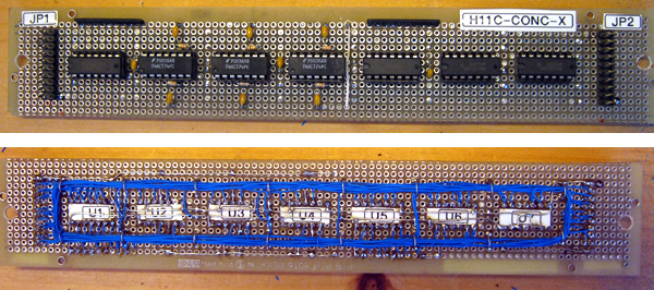
Hardware development on hold
6/19/2010
Debouncer board (H11C-CONC-X) was finished last night, being this the last hardware-related job until September. Hardware development is now on hold for the next two month.
Software and design related tasks, however, will continue; such as the production of the H1ASM assembler and the H1SIM simulator, and the re-design of the Master Controller board among others.
Reviewing the Instructions Set Architecture
06/20/2010
The current Instructions Set Architecture was designed nine months ago based on my early ideas about how instructions would be decoded using hardwired logic. I still think it's not a bad design, but it needs some adjustments and that's exactly what I am doing.
The new architecture relies, pretty much, on the same ideas, but it makes better use of bit-fields and it's better oriented to the decoding circuitry (yet to come). It is more rational, I think, and it also makes room for new instructions that I have in mind such as those for ALU operations with memory (not allowed by the current ISA) and increment/decrement instructions optimized for typical loops.
It is still pending how to produce long sequences such as the ones required for CALL and RET instructions (longer than 4 clock periods) but... I'm working on it.
The new (revised) Instructions Set is complete
06/26/2010
Finished to define and document the (revised) Instructions Set Encoding. It wasn't too hard but it was very tedious...
Also got to a solution for long sequences (instructions CALL, RET and INT) which take 8 cycles to execute instead of 1 to 4 cyles that all other instructions take.
Here is the resulting document:
http://www.armandoacosta.com/cpu/index.php?branch=576
Migrating to MS-DOS
06/27/2010
A few days ago I installed MS-DOS 6.22 on an old Pentium PC that I have and then copied to its hard drive my "glorious" probation of DOS stuff from my backup CDs. Needless to say that DOS is a lovely environment for old-fashioned tech people such as my self, so I got fascinated with the result.
What I love of working with DOS (rather than Windows or Linux) is the simplicity. You get things done quick and almost effortlessly; you have fewer choices so fewer things to worry about; you can focus on what you are doing with no distractions.
I was planing for C but the Microsoft Quick C ver 2 (QC2) that was once my war horse, were corrupted so for development I only have a copy of Borland Turbo Pascal 3.0... very limited but good enough for producing my assembler/simulator winning couple.
So it is decided: DOS will be the development environment for Heritage/1 software production. H1ASM will be rewritten in Turbo Pascal taking advantage of the good experience I had with the PHP implementation. The H1SIM simulator will also be written in Turbo Pascal... for DOS!
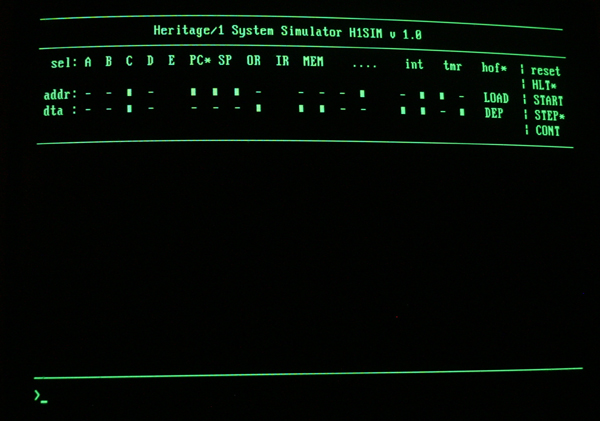
Working hard on the Simulator
7/8/2010
This simulator written in Turbo Pascal 3.0 proven easier than expected. In only six days (or nights...) of development it got to Fetch and Execute "real code" previously read into "memory" from a hex file.
I wanted it to look primitive, even more primitive than those programs that I used to write with Turbo Pascal twenty years ago. The text-only interface resembles the computer's console in a direct way, no fancy debugging commands have been added other than the ability to read a hex file from disk.
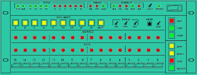
This primitive design has resulted in an intimate experience, very close to the machine being emulated which Console is expected to look more or less like this:
This program does not mimic the Heritage/1 exact circuits but only its behaviour. Hower, it resembles the hardware architecture at the block level, implementing in software the same solutions as in hardware. This match between software and hardware is giving me the oportunity to test those solutions on cold... which wasn't my initial intention, I have to confes...
Finished ISA review
7/15/2010
This simulator has proven to be a great "prove of concept" tool. It helped me to find inconsistencies in my Instructions Set that was more than happy to fix right a way.
Back to work
9/24/2010
I've taken this project back after a long pause and I've started by reviewing all of the "facts" most of them settled since many months ago. The architectural features are --I can see-- very mature at this point. Heritage/1 can definitely be described as a strict 16-bits "traditional" minicomputer based on single accumulator, single ALU, offering a --I would call it-- rich instructions set designed to execute simply and fast.
Features I really enjoy are the following:
- Instructions decoded by hardwired logic.
- Double-buffered registers.
- Not use of ROM
There are some features, however, that don't get to fit into the whole picture as for example the ability to disable the Timer by software (instruction DT: Disable Timer).
The idea behind the Timer was always the same it is still today: to assists a multiprogramming operating system in switching between processes. I've been always thought of the Timer as sort of "watch dog" sat there to make nearly impossible for a crashing process to hang the entire system... well, to try at least. So allowing routines to disable the Timer defeats its very purpose.
Today I decided to resolve the matter by getting back to the original idea that I've violated three month ago against my own sense of consistency. So, yes, I'm definitely removing instructions ET, DT from the Instructions Set as well as the TE flag (Timer Enabled) from the Flag's Register. Any solution for preventing critical-region code from being interrupted by the Timer's tic must be found within the OS design, not the CPU hardware.
It occurs to me, for example, that all system calls (issued asynchronically by processes) could wait in a "pending service queue" to be serviced later at "tic-time". Anyways, I'm not designing an Operating System yet so those issues will get actually solved in the future. For now I'm focusing in hardware design and I want it to be a clean one.
|