IntroductionHeritage/1 is a general-purpose stored-program 16-bits digital minicomputer designed to work similarly to those of the early 1970s. Circuits have been built using SSI/MSI integrated circuits of the 74HC00 series (HCMOS), being SRAM the only LSI chips employed. At present, the machine lacts ROM memory but plans exist for building such based on discrete diodes-matrix.
Design Phylosopy
A simple computer designed to taste old and serve well.
Minicomputer
"What we do today, tomorrow sounds old" --pointed out Ken Olsen in 1982 referring to Digital's effort to enter the personal computer market. I would add that obsolesce is not a bad thing for technologies that reached their momentum of glory at some point in history, and that's exactly the case of "minicomputers" back in the 1960s and 70s.
Most people today recall their first encounters with early personal computers unaware -in most cases- that computers started to be popular much before than that, possibly when they were attending elementary school. What actually introduced the computer to the popular culture was not the so called "personal computer" but those refrigerator-size monsters that back then were called "minicomputers".
Heritage/1 has been designed around that concept. It is not a "mainframe" because mainframes are designed to carry out heavy work loads and their design puts an emphasis on reliability (to which end they employ generous amounts of redundancy). It is not a "personal computer" either because it lacks a video monitor, a keyboard and a mouse.
Heritage/1 is a minicomputer and she has been designed to work exactly in that "classical" fashion. Any temptation to modern thought has been intentionally removed from the mind of the author. The modern concept of "fixed disk" is an example: back then, data (and software) did not reside "into the computer" (as part of it) but "outside the computer" supported by removable media such as tapes and removable disks.
Batch Processing
It is hard for modern people to put the PC experience aside in order to get into the minicomputers spirit. But even harder is to conceive a computational environment which is not interactive at all. Not being able to run a program by just entering its name as a command. Not entering data from the keyboard directly into the application's interface nor asking short question for getting immediate answers.
Computers, however, worked in "batch processing" for more than twenty years: from early 50s to long after UNIX were invented in 1972. Software and data were entered from files and results were obtained thought the printer after minutes (if not hours) of silent computing.
Today is hard to imagine such a work flow, specially while designing a homebrew minicomputer. It seems to be no excitement in writing programs that just read files and make printouts.
But that's precisely why I encounter "batch processing" to be a fascinating field for exploration. I consider it a mental challenge because it will require for me to rethink Computing all together up to the point that my current experience as a computer user is not use.
Time-Sharing
Time-Sharing (multi-user) is where the excitement becomes obvious. I suspect, however, that it's going to be extremely hard for me to produce a Time-Sharing system for Heritage/1. That is why I don't plan to attempt such a thing at present, not before I've gained some experience with system development in general.
Heritage/1 Design Phylosophy
The first idea behind Heritage/1 is to be a minicomputer. It has to do with punch and magnetic tapes, teletypes and video terminals. Culture can not be explained (otherwise it was Math) so I won't try to.
Some other ideas are the following:
1.- Meant to be useful (as minicomputers were at their time)
2.- Reasonable performance (no annoying waits)
3.- Simple architecture (no fancy features such as Virtual Memory)
4.- Data and software are "external" to the computer (no ROM, no Fixed Disk)
Techniques empoyed
This section describes some of the different techniques employed to design the Heritage/1 circuits.
Buffers instead of Muxes
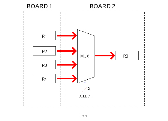
Multiplexers are usually employed to convey data from different sources into a single destination. Figure 1 shows an hypothetical example in which one of four registers (R1, R2, R3, R4) is selected to input a destination register R0.
If the sources and destination are placed in different boards as shown in figure 1, wiring could get expensive. For example, if each data path is 16-bits, then 64 wires would be required to interconnect the two boards.
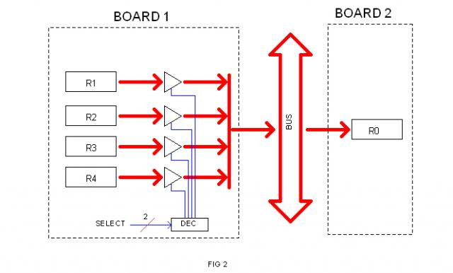
Figure 2 illustrates a different solution. The MUX in BOARD 2 has been replaced with four 3-State buffers placed in BOARD 1. Now the selection is done in the source, not in the destination. An external BUS has been used to interconnect the two (and possibly others) boards. Consequently, only 16 wires are required.
This technique not only saves wires (and connector's pins) but it also allows for a more flexible and modular design. For example, a second 4-registers board could be added at a later time without having to modify neither BOARD 1 nor BOARD 2.
Extensive use of Diodes
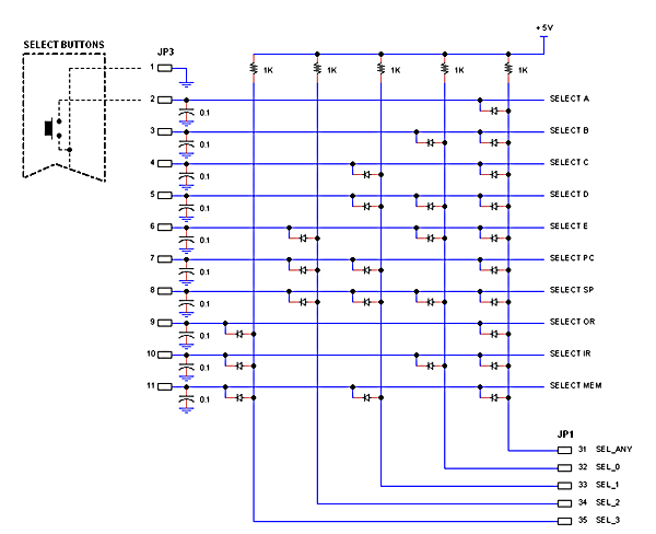
Diodes Logic (some times regarded as "Micky-Mouse Logic") has been employed along history since first generation of computers (1940s). The following diagram illustrates a typical use: keyboard encoder. This circuit encodes the "Data Select" buttons of the CPU Console.
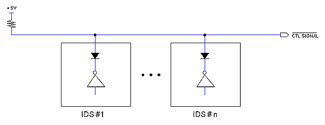
The image below illustrates another use of diodes in the CPU. As same control signals are generated in different Controller boards, a "Control Bus" (C-BUS) was employed to convey those. Then a wired-OR (actually built with diodes) was used to provide an inexpensive "distributed OR gate".
Hardwire Logic instead of Microprogramming
Heritage/1 decodes instructions using logic circuits, that is actual gates. This avoids the speed contraint imposed by microcode storage if Microprogramming were otherwise employed.
Decoding by pure logic is interesting since the design is made based on Boolean algebra rather than "intangible logic", allowing the designer to think as an electrical engineer instead of a programmer. It also matches the Heritage/1 design philosophy in the sense that "Software is external to the Machine" and as such it has to be loaded on a hardware that has full-started already.
In section Building sequences with combinatorial logic this techique is explained in general terms.
General Theory of Operation
Internally, the CPU works very similar to a clock's machinery. Nearly all internal activities consists of sequences of internal control signals. Some sequences are built automatically, others are built as instructed in the current instruction's operational code.
Control Signals
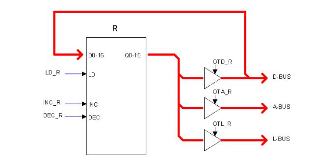
The figure below represents a typical Heritage/1 register as an example of a circuit being controled by internal control signals.
The circuit encapsulated into the box can latch a 16-bits word. It can also increment or decrement its content. Latched content is always available at the Q0-15 outputs but those are isolated from the buses by the mean of three 3-state buffers as shown.
Control signal LD_R makes the register to latch its inputs D0-15 which are connected directly to the D-BUS. Signals INC_R and DEC_R makes the content to increment or decrement respectively.
In order to expose the register's content to the D-BUS, signal OTD_R must be present. Similarly signal OTA_R makes the content available to the A-BUS and OTL_L, to the L-BUS. This later is the "lamps bus" which content is always shown in the Console's Data Lamps (LEDs).
The naming convention for control signals is: SIGNAL_RESOURCE as in LD_R (Load register R). Common prefixes are (among others):
LD_ Load (clock to latch)
OTD_ Output To Data (open buffer to D-BUS)
OTA_ Output To Address (open buffer to A-BUS)
OTL_ Output To Lamps (open buffer to L-BUS, the "lamps" bus)
INC_ Increment
DEC_ Decrement
All control signals are active low with no exception. This makes it easier to "OR-them" using diodes.
Sequences
The previous example makes it clear the need for sequences. For example, to move content from register B to register A, the following sequence is needed:
1.- Open register B to the D-BUS by activating the OTD_B signal.
2.- Load register A from the D-BUS by activating LD_A, while keep OTD_B active.
3.- Deactivate both OTD_B and LD_A.
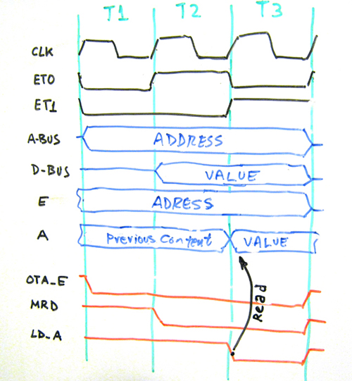
Sequences are synchronous with the computer master clock (CLK). A central counter named T-COUNTER (clocked by the master clock) generates two "encoded-time" signals named ET0 and ET1 respectively. Sequences are actually built by combinatorial logic using ET0, ET1 as inputs.
The four possible combinations for ET0, ET1 are conventionally named: T1, T2, T3, T4 as following:
ET1 ET0 T
----------------
0 0 T1
0 1 T2
1 0 T3
1 1 T4
----------------
The time diagram below illustrates the execute cycle for the instruction:
ldx a, e
This instruction reads the memory location pointed by register E, into register A.
The time diagram shows the sequence of control signals OTA_E, MRD, LD_A needed to execute the given instruction. MRD (Memory Read) is an external signal present in the U-BUS wired to open the memory chip buffers to the Data Bus.
As shown, signals activate and deactivate at CLK period intervals as result of changes in ET0, ET1. The master clock (CLK) is currently 4 MHz thus this particular sequence takes 750 ns to complete. The shortest sequence in Heritage/1 takes one clock period (250 ns); the longest takes eight (2 us).
As mentioned, all sequences are built from ET0, ET1. The only exceptions are of those built by the Console; this exception has been made in order to minimize dependencies since the Console is meant to be the ultimate resource to control de computer in case of failure.
Building sequences with combinatorial logic
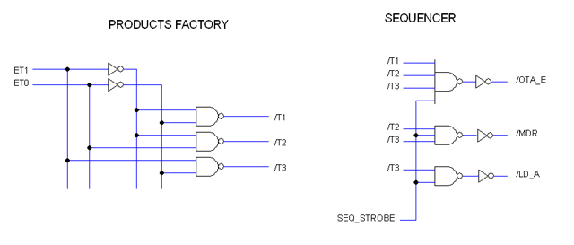
As an example, we will design a circuit to generate the sequence of previous section. The circuit will take signals ET0, ET1 as inputs to generate /OTA_E, /MRD, /LD_A as outputs.
Note: We use a forward slash (/) to denote logic inversion.
From the time-diagram on previous section we can directly deduct the equations. In order to make things simpler we will mentally invert the control signals OTA_E, MRD, LD_A so they will become active-high as opposite as shown in the diagram. The resulting equations are these:
OTA_E = T1 + T2 + T3
MRD = T2 + T3
LD_A = T3
Where T1, T2 and T3 are products of E0, E1 as following:
T1 = /ET1 * /ET0
T2 = /ET1 * ET0
T3 = ET1 * /ET0
The drawing below shows the resulting circuit.
The circuit on the left (Products Factory) obtains the required products T1, T2, T3. Notice that NAND gates have been employed instead of AND; the purpose of this is to be able to sum products using NANDs (applying De Morgan's Law) which is some times convenient in practice.
The circuit on the right (Sequencer) conveniently sum different products to obtain the different signals according to the equations being implemented. Notice that NAND gates have been employed instead of OR since they receive inverted signals as mentioned before. The NAND's outputs are then inverted because the intended signals are active-low as shown in the time-diagram on previous section.
A typical board builds more that one sequence, thus same products are reused among different sequencers. A single Products Factory is then employed to build all products involved whereas several Sequencers separately sum the required products as required.
Signal SEQ_STROBE actvivates the Sequencer in question. Needless to say that only one sequencer can be active at a given time in the entire CPU.
Decoding Instructions
Operational Modes and Syncrhronization
Managing Conditional Status
Managing Fault Conditions
External Architecture
Units
The Heritage/1 minicomputer consists of several units. Each unit is a rack-mount multi-cards frame with its own power supply and internal buses. Different configurations are possible by combining different units in a number of possible ways. They can all populate a single rack or arranged in different ones as needed.
Units communicate each others by the mean of a 39-lines bus called U-BUS. Externally the bus consists of two cables ended with D-SUB connectors (37-pins and 9-pins respectively). Cables plug to units in a daisy-chain fashion. The last unit in the chain requires to be terminated by the mean of a two terminator connectors.
Wires in the bus carry either signals or ground. No power is provided through the U-BUS.
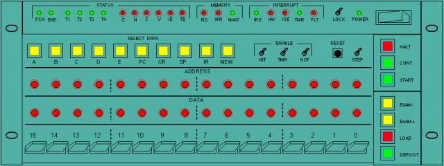
Console
The Console, possibly the most prominet component of the machine, is placed on the front of the Central Processing Unit (CPU) which is in turn the most important unit on the entire computer.
The Console is used for operating the machine and also for debugging developing software. It relies on five boards to function; one (H11R-LARLDR) plugs to the Backplane along with the rest of CPU cards; the other four (H11C-CONC, H11D-CONB and two H11D-CONL) are located within the Console assembly.
As a whole, the Console is considered a "controller" as it runs sequences on its own in response to commands issued by the Operator from the Console's buttons and switches. Know however that Console sequences can only run when the computer is in Halt mode, as explained in the Operator's Manual.
Main Memory
Main memory is located in a dedicated unit called "Core Unit". Modern memory chips occupy little space but further expansion is expected (such as building ROM based on diodes-matrixes, support for Virtual Memory etc.) hence the extra space needed.
Memory is wired in 16-bits words (as opposite of 8-bits bytes). This means that a given address allways referres to a memory location which is 16-bits wide. A number of instructions have been provided for manipulating bytes within words but that is only once the content has been read into a CPU register.
At present, the 64 Kwords addressable space is "real", that is no support for Virtual Memory yet exists.
Peripherals
Peripheral's controllers are built as Units. For example, the "COMM Unit" contains a number of UARTs for RS-232 ports accessible from its rear panel. Different controllers can be housed within the same Unit for convenience. For example, an IDE hard drive could be placed in the COMM Unit in order to save space.
In Heritage/1, all peripherals are memory mapped. This implies that device's registers and buffers occupy a portion of the overall (64 Kwords) addressable space. These memory chips (wired as dual-port memory) and associated circuitry reside in the peripheral's Unit. The address range is manually set by the mean of DIP switches located in the unit in question.
Expansion
The Heritage/1's topology puts no limit to expansion. New units can be designed, built and added to the existing configuration as required.
An interesting area for expansion is Virtual Memory. Originality the machine does not provide any support for that; however, it can potentially be implemented in the Core Memory Unit without having to modify the CPU at all.
Detailed information and guidance for designing new Units are provided in this Manual.
Interrupts Architecture
The Heritage/1 CPU can accept up to 64K non-vectored hardware interrupts while only three control lines are employed for negotiation. Nested interrupt service routines (ISR) are possible according to priorities.
The CPU also accepts 256 vectored software interrupts which vectors are shared with interrupts generated by the CPU itself such as Fault and Timer.
Interrupt Controller
There are two moments in the life of an interrupt: Negotiation and Service. During the first, the CPU and the interrupter device negotiate the use of the buses until finally the ISR address is passed from the device to the CPU. The second moment starts when the CPU passes control to the ISR (PC loaded with the ISR address) and finishes when the ISR returns and control is passed back to the interrupted routine.
During interrupt negotiation, the Interrupt Controller takes over; this is coordinated by mean of status signals S0, S1 present in the Status Bus (S-BUS).
Once the ISR address has been obtained, the Interrupt Controller saves the Program Counter (PC) and Flags register (F) to the stack. Finally it loads the PC with the ISR address and rises an End Of Interrupt (EOI) signal so the next Op Fetch cycle can take place over the interrupt service routine.
External Interrupts
Interrupter Peripherals don't provide "vectors" but instead the actual address of the Interrupt Service Routine (ISR). Therefor, up to 64K different external interrupts are possible.
External interrupts can be enabled (EI) and disabled (DI) by software. When the interrupt occurs, the CPU disables interrupts automatically. Every ISR is expected to enable interrupts back to allow for nested interrupts service.
 Topology Topology
Three control lines are present in the External Control Bus for serving external interrupts: IRQ (Interrupt Request), IAK (Interrupt Acknowledge) and ISE (Interrupt Service End). These lines connect to all devices in Daisy Chain so any interrupter device can open the lines to avoid further propagation along the chain. This way, priority gets established by the "proximity" of the device to the CPU.
Interrupt life-time
Here is the sequence of events during an interrupt.
0.- Initially, no interrupt is being requested. IRQ, IAK and ISE lines are inactive and the buses are being used by the CPU to run the current routine.
1.- Some DEVICE wants to interrupt. The first thing it does is to open the chain to avoid IRQ and IAK signals to propagate further along the chain. Then, it signals the CPU for attention by activating the IRQ line.
2.- The CPU finishes the current instruction, then disables interrupts (DI) and signals the DEVICE to provide the interrupt address by activating the IAK signal. The device is expected to release the address immediately (within a clock cycle); IAK is actually a "read" signal similar to "Memory Read" (MRD).
3.- The DEVICE provides the interrupt address which is read into the the Operand Register (OR) during the next clock cycle. The CPU deactivates IAK to notify the DEVICE.
4.- When the DEVICE notices that IAK is not longer present, it releases the Bus and drops the IRQ signal.
5.- The CPU can now utilize the buses so it saves PC and F to the Stack, then transfer OR to PC for passing control to the interrupt service routine (ISR). This routine is expected to enable interrupts back (EI).
6.- When the Interrupt Service Routine reaches the RETI instruction (return from interrupt), the CPU recovers F and PC from the stack for passing control back to the previous routine. Then, it rises the signal ISE (Interrupt Service End).
7.- Until this moment, the DEVICE had kept the chain open so less priority devices could not interrupt. Now, it utilizes the ISE signal to close the chain back. If a less priority device had issue an interrupt request already, it will now reach the CPU for attention.
NOTE: The ISE signal is a low-going pulse, half-a-clock wide. The interrupter device is expected to close the chain with the rise edge of the puse so the pulse itseft don't propagate further.
If you "run" this sequence with multiple devices interrupting at the same time, you will see how different ISRs nest each another observing the priorities set by device proximity.
Interrupter Device Requirements
Interrupter Devices must be designed to follow the above protocol. According the Heritage/1 design principles, LSI technology (such as programmable UART chips, PLAs etc) can NOT be employed to implement Device Controllers; the logic involved, however, is very simple.
The ISR address to provide is set with DIP switches standing behind a 3-state buffer (two 74HC244). The IAK signal does nothing but opening this buffer to the Data Bus.
The Daisy Chain is opened and closed with simple gates, thought the logic also involves a flip-flop to keep track of the "IRS running" state, which changes back upon ISE signal is received.
Other buffers and registers will surely needed for specific operations. The main idea is that the CPU will treat peripherals as memory locations and will access them "at memory speed". Delays associated with internal mechanisms (such as reading from magnetic tape to internal buffer) must take place when the peripheral is not being accessed, that is concurrently with normal CPU operations.
Internal Interrupts
Internal interrupts can be generated by Software, from the Timer or when a Fault condition is detected. All internal interrupts are vectored (8-bits vector).
Vectors occupy all together the first 256-words block of the addressable space: 0x0000-0x00ff. Vector 0 is at 0x0000, vector 1 is at 0x0001 and so on. Each location contains the actual address of the corresponding Interrupt Service Routine.
Fault
Certain circuits in the CPU are capable of detecting fault conditions such as illegal instruction. When a Fault is detected, the Interrupt Controller is notified. It reacts by taking control of the CPU for saving PC and F to the stack, then loading the Program Counter (PC) with the content of memory location 0x0001. This behavior, however, can be changed from the computer Console so the computer simply halts on Fault.
This interrupt is not affected by the DI instruction.
Timer (Computer "tic")
The Timer is located in the Interrupt Controller. It is a simple counter triggered from the System Clock and wired to produce interrupts at long intervals (for example, 1 ms) set by DIP switches.
The address for the Timer Service routine is indicated in memory location 0x0000. When the timer interrupts, the Interrupt Controller loads the Program Counter (PC) with the content of that memory location (after have saved PC and F to the Stack).
This interrupt is not affected by the DI instruction but it can be disabled from the Console.
Software Interrupt (INT)
The instruction INT generates a Software Interrupt. This instructions takes one argument (embedded within the operational code) which is the 8-bits interrupt vector.
Notice that address 0x0000 is the one for the Timer and 0x0001 is the one for Fault. This means that both Timer and Fault interrupts can be simulated by software (INT 0 and INT 1 respectively).
Interrupt Priorities
Priorities are in this order:
1.- Timer
2.- Fault
3.- External
4.- Software
|