ContentThis section describes the computer's hardware in a generic, introductory way.
The Instructions Set Architecture (ISA) is covered in details.
General description
HER/12 is a parallel registers-based 12-bit mini-computer built from discrete Small and Middle Scale of Integration (SMI, MSI) integrated circuits of the 7400 series. It does not employ LSI components other than semiconductor Random Access Memory (RAM) chips.
The machine consists of the CPU equipment and up to 16 external peripherals connected to the CPU via I/O channels (as opposite of external bus).
The CPU contains the main memory, organized in 4096 words of 12 bits each. Memory expansion is possible through RAM-DISK peripherals connected to channels. RAM-DISKs are block devices with maximum capacity of 256 Mwords.
Other peripherals could be: printers, punch tapes, magnetic tapes, serial ports, D/A and A/D, GPIO, real-time Timers and many others.
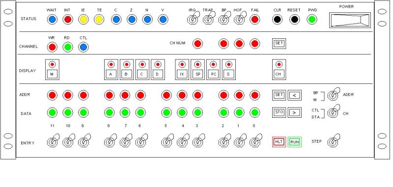
The CPU is operated by the mean of a Console located in the front of the CPU. Software and data can be entered into memory either manually (using the Console) or from external support such as punch tape or magnetic tape.
Registers and Memory
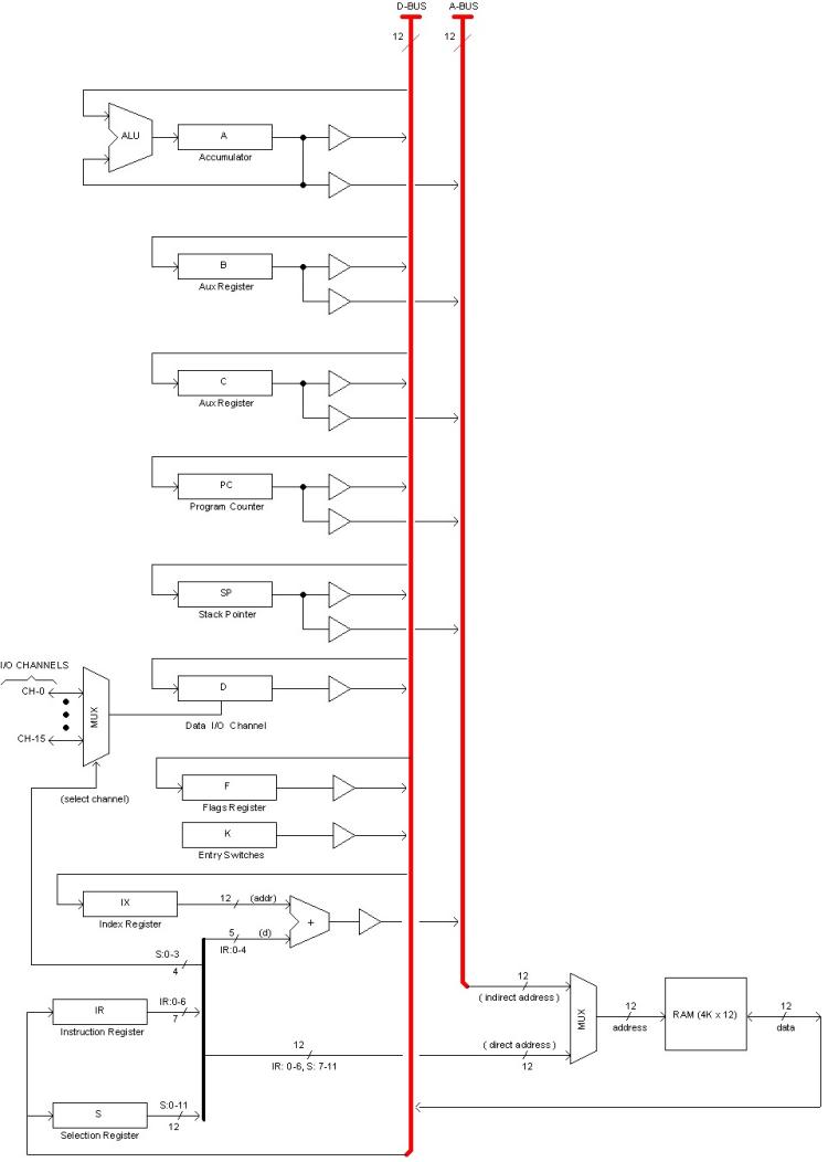
Memory is part of the CPU equipment. It is 4K x 12 bits, not extensible. Registers are implemented in the CPU equipment as well. The following diagram shows the CPU registers, the Memory, and how they connect to the Data (D-BUS) and Address (A-BUS) internal buses.
All registers are 12-bits.
The small triangles represent 3rd-state buffers isolating registers outputs from the buses. A typical register can output to both D-BUS and A-BUS; in the later case, the register is acting as a pointer to memory providing an "indirect address". Only one register can open to the same bus at the same time.
Register A acts as accumulator holding the result provided by the Arithmetic and Logical Unit (ALU), which is a combinational circuit capable of performing 16 different operations including 2's complement and BCD arithmetic. The default operation is "pass-through", in which case the accumulator functions as a general purpose register.
Auxiliary (general purpose) registers B, C and D are mostly intended to serve as pointers to memory although they can be used to hold temporary data as well.
PC, SP, IR and F are the Program Counter, Stack Pointer, Instruction register and Flags register, respectively.
Register K (read-only) is a direct input from the Console Entry Switches.
Register S holds the current channel number and the current memory page as explained later. In the diagram, S:7-11 contributes a "page number" to a 12-bits direct address, being the other 7 bits supplied by the instruction's code (IR:0-6). This is explained later in section "Paged Memory".
Index register (IX)
IX is the "index register". It provides an address with displacement intended for programs to access structured data in memory. The displacement is given by bits 0-4 of the instruction's code. Both numbers are summed out using an adder circuit to provide an effective 12-bits address IX+d as shown in the diagram.
Status Registers
Status registers (PC, F, S) define the current state of the machine as programs execute. That is why interrupts take care of saving PC, F and S content to the stack before branching so the machine state is preserved for the interrupted program upon return. The same is also true for CALL instructions.
 Program Counter (PC) Program Counter (PC)
When button RUN is pressed in the Console, the CPU starts a "Opcode Fetch Cycle". The memory cell which address is currently indicated by PC, is read into register IR. Then the instruction is decoded and executed, and the Program Counter is incremented appropriately.
Once the instruction is complete, a next Opcode Fetch Cycle is initiated and so on, until the machine is halted some how.
Flags register (F)
Flags bits indicate whether the last instruction resulted in a Carry (C), Zero value (Z), Negative value (N) or Overflow (V) in the target register. All ALU operations (except "pass-through") affects flags, as well as transfer and increment/decrement instructions. Writing to memory does not affect flags.
When pushed or popped to/from the Stack, the Flags register is treated as a monolithic 12-bit register, but its real implementation is different. For one part, only 8 bits are implemented (the 4 most significant bits always read zero). For the other part, flags need to be set/reset individually.
The register F also holds the current ALU function. This is latched as a result of ALU instructions having the LOCK keyword in assembly language (see section "SubClass 010: ALU" in "Instructions Set Architecture").
The following table shows the F register format:
bit designation descript
--------------------------------------------------------------------
0 f0 ALU function
1 f1 ...
2 f2 ...
3 f3 ...
4 V Overflow flag (result rolled-over to zero)
5 N Negative flag (most significant bit of result is 1)
6 Z Zero flag (all bits in result are zero)
7 C Carry flag (ALU result did not fit in 12 bits)
8 0 (not used)
9 0 (not used)
10 0 (not used)
11 0 (not used)
--------------------------------------------------------------------
Selection register (S)
The Selection register (S) holds the current memory page number (5 bits) and currently selected channel number (4 bits). The remaining 3 bits are not used and always read zero.
bit designation descript
------------------------------------
0 c0 channel number
1 c1 ...
2 c2 ...
3 c3 ...
4 p0 memory page
5 p1 ...
6 p2 ...
7 p3 ...
8 p4 ...
9 0 not used
10 0 not used
11 0 not used
-------------------------------------
Hidden registers
Hidden registers are those not accessible to the programmer in the sense that there no instructions to read or write them directly.
Register G
G is a name given to a collection of unrelated individual flip-flops:
FF Meaning when set
---------------------------------
IE interrupt is enabled
TE fail trap is enabled
Fail fault condition detected
----------------------------------
This register is cleared on reset, resulting in a halted machine with no pending conditions.
Lamps Address Register (LAR)
The LAR register latches the word being displayed in the Console ADDR display. Actually, those lamps are fed from LAR's outputs.
When the machine is halted, LAR provides the address to actually address the memory in operations such as examining and altering memory content.
During normal program execution, LAR is updated (latched) for each machine cycle.
Lamps Data Register (LDR)
Similar to LAR, the Lamps Data Register (LDR) holds the DATA display reading.
LDR register is fed from the Lamps Bus (L-BUS) which is fed in turn from the selected register or memory (M) as the operator selects so in the Console.
When the machine is in normal program execution, if M is selected, LDR is updated for each memory read or write cycle. If a register is selected instead, LDR remains open passing to the Display the L-BUS content (that is, the selected register).
When the machine is halted, LDR is the destination of memory reading cycles made by the Console circuitry when the Operator examines memory content.
Break Point Register (BPR)
The BPR register stores a break point set by the Operator.
When the BP/M switch is in its up position, BPR output feeds the ADDR display (instead of LAR). In this condition, BPR will latch the K register content (Entry Switches) if the SET button is pressed, being this the way for the Operator to set the Break Point in the machine.
Paged Memory
In order to provide direct addressing in a single-word instruction, the 4K memory space has been broken into 32 pages, 128 words each. The current page number is held in a 5-bits field of register S. The offset (7-bits) withing the page is encoded in the 12-bit instruction's op code.
This way, direct addressing instructions do not address the entire memory but only the current page. Another instruction allows to switch to the desired page. This apparent inconvenience can be camouflaged in assembly language with pseudo-instructions that accept 12-bits addresses to automatically insert a page-switch instruction if necessary.
In the diagram, we can see how bits from registers S and IR are combined to build the 12-bits direct address.
Instructions Set Architecture (ISA)
Addressing Modes
The architecture explained above yield to the following addressing modes.
Mode Example Descript
--------------------------------------------------------------
Register ldr A, B r1:= r2
Immeditate ldi A, value r := value
Direct ldd A, address r := [page + address]
sto A, address [page + address] := r
Page-Zero Direct ldz A, address r := [address]
stz A, address [address] := r
Indirect ldx A, B r1:= [r2]
stx A, B [r2]:= r1
Indirect w/ auto-inc ldy A, B r1:= [r2], r2++
sty A, B [r2]:= r1, r2++
Index ldix A, d r := [IX + d]
stix A, d [IX + d] := r
Stack push A SP--, [SP]:=r
pop A r:=[SP], SP++
---------------------------------------------------------------
In Direct Addressing instructions, "address" is an 7-bits offset within the current memory page as explained in previous section.
Page Zero addressing allows direct access to memory locations in "page zero" (000H-07FF) independently from the page number currently held in S. This is an important feature because access to HER/12 memory is as fast as accessing registers, so Page Zero effectively provides 128 extra "registers" to the programmer.
Both Direct and Page Zero addressing are limited to registers A, B, C, PC.
Indirect Addressing is implemented by simply opening the desired pointer register to A-BUS.
Indirect with auto-increment is same as Indirect, only that the pointer register is post-incremented. This is convenient to software when looping through a memory buffer.
Indexed Addressing allows to point memory structure with IX, then get access to different fields within the structure by the mean of a 5-bits displacement (d).
Encoding
The instruction's opcode and operands are encoded together in a single 12-bits word. The only exception is Immediate Addressing in which case the operand (value) is given in a second word following the opcode.
In the following sections, the notation r:= [ address ] means: copy the memory location which address is address, to register r. Expressions into curly braces represent mnemonics.
Instruction Classes
The three most significant bits of the opcode represents the "Instruction's Class", a code that selects the appropriate decoding circuitry. Remaining bits are encoded depending of the Class.
Classes are the following:
bin dec Descript Mnemonics
----------------------------------------------------------------------
000 0 Page Zero direct load ldz
001 1 Page Zero direct store stz
010 2 Direct addressing load ldd
011 3 Direct addressing store sto
100 4 Register or Immediate addressing ldr, ldi
101 5 Indirect with or without auto-inc ldx,stx,ldy,sty
110 6 Indexed (r <--> IX+d) ldix,stix
111 7 Sub-Classe (all others)
----------------------------------------------------------------------
CLASSES #0, #1: Page Zero
000 rr aaaaaaa ; register 'rr' <-- [ 00000 aaaaaaa ] { ldz r, addr }
001 rr aaaaaaa ; register 'rr' --> [ 00000 aaaaaaa ] { stz r, addr }
Direct addressing is limitted to registers A, B, C and D.
In the mnemonic, addr represents the 7 least significant bits of the address
being bits 8-11 all zeros.
CLASSES #2, #3: Direct
010 rr aaaaaaa ; register 'rr' <-- [ ggggg aaaaaaa ] { ldd r, addr }
011 rr aaaaaaa ; register 'rr' --> [ ggggg aaaaaaa ] { sto r, addr }
Direct addressing is limitted to registers A, B, C and D.
The 5-bits string 'ggggg' is the current page number held in register S.
In the mnemonic, addr represents and offset of 7 bits withing the current page.
CLASS #4: Register and Immediate addressing
100 rrr p00 sss p=0 => rrr <-- sss ; Register addressing { ldr r1, r2 }
p=1 => rrr <-- value ; Immediate (sss ignored) { ldi r, value }
In the case of Immediate addressing (p=1), the operand (value) is given
in the word following the opcode.
CLASS #5: Indirect with or without auto-inc and read/write channel indirect
Load/Store to register:
101 rrr 0ip xxx p=0 => rrr <-- [xxx] ; Load indirect { ldx r, x }
p=1 => rrr --> [xxx] ; Store indirect { stx r, x }
i=1 => Increment xxx after transfer { ldy r, x }{ sty r, x }
Read/Write to selected channel:
101 000 10p xxx p=0 => [xxx] <-- Channel Data path ; read data indirect { ldch x }
p=1 => [xxx] --> Channel Data path ; write data indirect { stch x }
101 000 11p xxx p=0 => [xxx] <-- Channel Control reg ; read ctl indirect { ldct x }
p=1 => [xxx] --> Channel Control reg ; write ctl indirect { stct x }
These last four instructions provide the only way to access peripherals by software. Transfer is always indirect between Memory and the selected channel, using any of the suitable register as a pointer.
CLASS #6: Indexed
110 rrr pdd ddd p=0 => rrr <--[IX+ddddd] ; Load indexed { ldix r, d }
p=1 => rrr -->[IX+ddddd] ; Store indexed { stix r, d }
CLASS #7: Class Extensions (SubClasses)
Class 7 instructions constitute class extensions (or SubClasses). The subclass number is given in bits b6-8 of the opcode, being b9-11 = 111.
111 ppp --- --- ; ppp is the "sub-class" number
Depending of the SubClass, the instruction is encoded as following:
SubClass 000: Control
111 000 000 000 halt Halt the computer
111 000 000 001 di Disable interrupts
111 000 000 010 dt Disable trap
111 000 000 011 ?
111 000 000 1.. ?
111 000 001 000 ?
111 000 001 001 ei Enable Interrupts
111 000 001 010 et Enable trap
111 000 001 011 ?
111 000 01. ... ?
111 000 10. ... ?
111 000 11. ... ?
subClass 001: Set Page or Channel
111 001 0gg ggg ; Set page ggggg { setp page }
111 001 10c ccc ; Set channel cccc { setch chn }
SubClass 010: ALU
111 010 rr ffff
This instruction sets the ALU with the function 'ffff', then transfers register rr into A
(if pertinent) to finally latch A with the result.
Bits 'rr' are coded as following:
rr means:
--------------------
00 transfer from A
01 transfer from B
10 transfer from C
11 ---lock ALU---
--------------------
The last (11) is a special case in which no result is obtained at that time. A second instruction
is required to complete the operation. It works as following:
If rr=11, 'ffff' is latched into register F, locking the ALU operation this way.
The next instruction is expected to be a transfer to A. Since the ALU is locked with the
function, the operation is effectively completed this time, obtaining the result in A.
The ALU is automatically unlocked at the end of this second instruction.
It follows from the above explanation that ALU instructions operates in two forms:
DIRECT FORM (rr < 11):
The operation is performed in that very instruction, but only registers A, B, C can be used
as source for the operand.
Example:
ADD B ; A:=A+B
DELAYED FORM (rr = 11):
The operation is locked and completed in a second instruction that can be any having register
A as destination. This allows to perform ALU operation using any addressing mode available to
register A.
Example:
ADD LOCK ; Special assembly keyword 'LOCK' indicates DELAYED FORM
LDD A, addr ; A:=A+[addr]
If the instruction following ADD LOCK is not a transfer to A, the operation is lost
since 'ffff' is unlocked automatically at the end of the second instruction.
This perhaps inconvenient implementation of ALU instructions can be camouflaged in Assembly
language with pseudo-instructions. The Assembler would insert the second transfer instruction
as appropriate.
Examples of pseudo-instructions:
ADDX B ; A:=A + [B]
ADDI value ; A:=A + value
ALU function (ffff) encodes as following
ffff Meaning
-------------------------
0000 => pass through
...
(pending design)
...
-------------------------
SubClass 011: Branching
111 011 pq1 ccc ; Conditional jump, call or return
111 011 pq0 000 ; Unconditional jump, call or return
p=0 => jump
p=1 => call
q=1 => return
ccc (condition) can be: mnemonic
---------------------------------------------------------------
000 flag Z=1; zero jz addr { or cz, or rz }
001 flag C=1; carry jc addr { similar to above }
010 flag N=1; negative jn addr ...
011 flag V=1; overflow jv addr
100 flag Z=0; non zero jnz addr
101 flag C=0; non carry jnc addr
110 flag N=0; positive jnn addr
111 flag V=0; no overflow jnv addr
---------------------------------------------------------------
Mnemonics for unconditional branching are:
jp addr
call addr
ret
Call instructions save registers PC, F and S to the stack before branching.
Return instructions pops registers S, F and PC from the stack before branching back.
NOTE:
Conditional branching is always immediate (address in second word operand).
You can implement unconditional jump with other addressing modes by simply
transferring an address to the PC, as in the following examples:
ldr PC, A ; PC:=A, useful for computed branching.
ldix PC, ptr ; PC:=[IX + ptr ], say that 'ptr' is a pointer to function
; stored as member of a structure being pointed by register IX.
SubClass 100: Stack
111 100 000 rrr ; { push r }
SP is decremented before transferring [SP]:=rrr
111 100 100 rrr ; { pop r }
SP is incremented after transferring rrr:=[SP]
Subclass 101: Increment / Decrement
111 101 00p rrr
p=0 => register rrr is decremented { dec r }
p=1 => register rrr is incremented { inc r }
SubClass 110, 111: Call Page Zero
111 11a aaa aaa
This instruction calls a subroutine which address is a pointer in Page Zero.
Example:
callz 21; --> 111 110 010 001 (21 is Octal).
The content of memory cell at address 0021 is a pointer to the actual routine being called. Before passing control to the subroutine, the instruction pushes registers PC, F, S to the stack.
Notice that the first 16 addresses of Page Zero are meant to content pointers to hardware interrupts routines, following by a pointer to the Trap routine (address 20 octal). The instruction callz instruction is kind of "Software Interrupts". Address 21 (octal) is a good place for the first of such software interrupt routines.
Also notice that we can use callz to simulate a hardware interrupt by just calling an existing ISR.
Registers Codes
Registers are encoded in instructions as following:
000 A
001 B
010 C
011 D
100 IX
101 SP
110 PC
111 K Console Entry Switches (read-only).
Instructions Set Summary
==============================================================================================
proj HERSIM -- ISA summary
==============================================================================================
Operational Code Mnemonic Description Cy Flags
----------------------------------------------------------------------------------------------
000 rra aaa aaa ldz r, addr Load page zero r= [000 00a aaa aaa] 1 ZN
001 rra aaa aaa stz r, addr Store page zero [000 00a aaa aaa]=r 1 ----
010 rra aaa aaa ldd r, addr Load direct r=[ppp ppa aaa aaa] 1 ZN
011 rra aaa aaa sto r, addr Store direct [ppp ppa aaa aaa ]=r 1 ----
----------------------------------------------------------------------------------------------
100 rrr 000 sss ldr r, s Register r=s
100 rrr 100 000 ldi r, value Immediate r=[PC+1]
----------------------------------------------------------------------------------------------
101 rrr 000 xxx ldx r, x Load indirect r=[x] 1 ZN
101 rrr 001 xxx stx r, x Store indirect [x]=r 1 ----
101 rrr 010 xxx ldy r, x with auto-inc r=[x], x++ 1 ZN
101 rrr 011 xxx sty r, x with auto-inc [x]=r, x++ 1 ----
101 000 100 xxx ldch x Read channel indirect [x]=channel 2 ----
101 000 101 xxx stch x Write channel indirect channel=[x] 2 ----
101 000 110 xxx ldct x Read channel control register indirect 2 ----
101 000 111 xxx stct x Write channel control register indirect 2 ----
----------------------------------------------------------------------------------------------
110 rrr 0dd ddd ldix r, d Load indexed r=[IX+d]
110 rrr 1dd ddd stix r, d Store indexed [IX+d]=r
----------------------------------------------------------------------------------------------
111 000 000 000 halt Halt the computer
111 000 000 001 di Disable interrupts
111 000 000 010 dt Disable trap
111 000 000 011 ?
111 000 000 1.. ?
111 000 001 000 ?
111 000 001 001 ei Enable Interrupts
111 000 001 010 et Enable trap
111 000 001 011 ?
111 000 01. ... ?
111 000 10. ... ?
111 000 11. ... ?
----------------------------------------------------------------------------------------------
111 001 0gg ggg setp g Set Page
111 001 10c ccc setch c Set Channel
----------------------------------------------------------------------------------------------
111 010 rrf fff ALU (--- pending design---)
111 010 11f fff ALU LOCK (--- pending design---)
----------------------------------------------------------------------------------------------
111 011 000 000 jp address Unconditional jump
111 011 000 ... ?
111 011 001 000 jz address Jump if Zero
111 011 001 001 jc address Jump if Carry
111 011 001 010 jn address Jump if Negative
111 011 001 011 jv address Jump if Overflow
111 011 001 100 jnz address Jump if Not Zero
111 011 001 101 jnc address Jump if Not Carry
111 011 001 110 jnn address Jump if Positive
111 011 001 111 jnv address Jump if Not Overflow
111 011 010 000 ret Unconditional return
111 011 010 ... ?
111 011 011 000 rz Return if Zero
111 011 011 001 rc Return if Carry
111 011 011 010 rn Return if Negative
111 011 011 011 rv Return if Overflow
111 011 011 100 rnz Return if Not Zero
111 011 011 101 rnc Return if Not Carry
111 011 011 110 rnn Return if Positive
111 011 011 111 rnv Return if Not Overflow
111 011 100 000 call address Unconditional call
111 011 100 ... ?
111 011 101 000 cz address Call if Zero
111 011 101 001 cc address Call if Carry
111 011 101 010 cn address Call if Negative
111 011 101 011 cv address Call if Overflow
111 011 101 100 cnz address Call if Not Zero
111 011 101 101 cnc address Call if Not Carry
111 011 101 110 cnn address Call if Positive
111 011 101 111 cnv address Call if Not Overflow
----------------------------------------------------------------------------------------------
111 100 000 rrr push r SP--, [SP]=r
111 100 100 rrr pop r r=[SP], SP++
----------------------------------------------------------------------------------------------
111 101 000 rrr dec r r--
111 101 001 rrr inc r r++
----------------------------------------------------------------------------------------------
111 11a aaa aaa callz addr Call Page Zero
I/O Architecture
Every peripherals connects to the CPU by the mean of a circuit called "Channel". The term has been borrowed from early IBM main frames, only that those were based on smaller dedicated computers (such as IBM 1401) whereas HER/12 channels solely provides a connection between the peripheral and the CPU buses, with no intelligence at all.
Up to 16 channels are supported but only one can connect to the CPU buses at a given time; that is said to be the "selected" channel. Selection can be made by software during normal program execution or manually by the mean of the Console when the computer is halted.
Data transfer is always between the selected channel and memory, using indirect addressing. The channel never reads or writes directly to a register.
Communication with peripherals is always initiated from the CPU. Peripherals can, at the most, assert interrupt signals to get CPU attention.
Assumptions about Devices
The device is expected to have at least two 12-bits internal registers:
DATA and CONTROL.
DATA holds the data to be transferred in one direction or the other;
CONTROL reports status and accepts commands. A bit (SEL) supplied
in the channels determines whether the dialog is from/to the DATA or
the CONTROL register.
The word length can be less than 12; for example, a Terminal device
will possibly have only 8 bits data path. In those cases, the device
must accommodate the used bits in the least significant portion of
the word, padding the rest with zeros.
Devices can also have other registers, but those would not be addressable
by the channel. Some sort of addressing via the CONTROL register would
be required in such cases.
The device accepts signals RD, WR to synchronize data transfer. It also
asserts an interrupt signal (INT) when it feels appropriate and accepts
an acknowledge signal (ACK) from the channel.
Devices can also synchronize by using a WAIT signal. When active, the
CPU delays the read or write cycle waiting from the device to complete
its part.
Channel Signals
The following signals are available to the peripheral in the channel.
Signal In or Out Descript
-----------------------------------------------------------------------
OL I Device Online
D0-11 I/O Data from/to either CONTROL or DATA register.
SEL O Select device register (0:DATA, 1:CONTROL).
RD O CPU reads from selected device register.
WR O CPU writes to selected device register.
INT I Device requires attention.
ACK O CPU acknowleges the interrupt.
WAIT I Hold the RD/WR cycle.
RST O Reset signal
The OL bit indeicates whether the device is "Online". This condition is stablished manualy by the operator of the device. The CPU refrains from accessing the device when the OL bit is clear.
Data path is 12 bits though some peripherals (example, a terminal) may use a shorter path in which case it must pad unused bits with zeros.
SEL is normally 0 to select the peripheral's data path (DATA register); it becomes 1 to select the peripheral's CONTROL register instead.
RD and WR are used to synchronize data exchange. When reading, the CPU pulls RD down to request data; in response, the peripheral must output the 12-bits data word in D0-11. When writing, the CPU writes the data in D0-11, then pulls WR down; in response, the peripheral must read D0-11 into its
internal DATA register.
INT is held down by the peripheral to request CPU attention. This line must be held until line ACK becomes active.
ACK is activated (down) by the CPU to acknowledge the interrupt. In response, the peripheral must release INT and get ready for data transfer. Most likely the CPU will perform a read operation on the CONTROL register to learn the nature of the request.
Some devices might be fast enough so not to require interrupt synchronization but slow, still, compared to the CPU speed; in those cases, the WAIT signal is used. When WAIT is down, the read or write cycle freezes waiting for the peripheral to complete its part. The peripheral must activate this signal as soon as the RD or WR signal is detected, hold it for as long as required, then release it to finish the operation. In response to WAIT release, the CPU completes its part: either latching the read data or disconnecting the channel from the D-BUS.
The WAIT signal can not be monopolized indefinitely which would cause the entire machine to freeze because of a defective peripheral. A time out of 32 clock cycles (2 micro seconds aprox) prevents this from happening. If the WAIT signal is held by that long, the I/O operation resumes and the WAIT signal is ignored by other 32 clock cycles. An alarm condition is raised to notify the anomaly.
RST is the master reset signal affecting the CPU and all devices. It is opt to the device to pay attention to this signal.
Interrupts
A device interrupts the CPU using the interrupt line (INT) located in
the channel it is connected to.
All INT signals coming from all channels go to the Interrupt Controller
circuit. A priority encoder provides a 4-bits code of the interrupting
device (matching its channel number) and takes care of priorities in case
of simultaneous request: channels with smaller numbers take priority.
The interrupt signal is sampled at the end of each instruction cycle,
just before fetching next instruction's op-code. If active, the interrupt
is serviced instead of performing the op-code fetch.
Servicing the interrupt implies the following:
Registers PC, F and S are pushed to the stack, channel switched to that of
the interrupting device, and the appropriate interrupt service routine (ISR)
is called. The sixteen 12-bit addresses of those routines are expected to be
at the top of the memory space:
000: ISR0_ADDR
001: ISR1_ADDR
...
00F: ISR15_ADDR
That address is loaded into the Program Counter (PC), the ACK signal is
asserted in the interrupting channel and interrupts are automatically
disabled to avoid unwanted nested interrupts.
The next opcode fetch cycle takes place on the corresponding ISR.
The ISR finishes with a return instruction. That instruction automatica-
lly pops S, F and PC from the stack, returning control to the interrupted
program. IRS routines are expected to enable interrupts back before
returning.
Inter-Device communication
Inter-devices communication is possible, it can be implemented in the device per se, but the CPU brings no support for that.
Implementing inter-device communication between a tape drive controller and a RAM-DISK device, for example, could provide some sort of Direct Memory Access (DMA), but, again, that would be in the rein of device's design, the CPU provides nothing to support such a thing.
|