ContentThis book contains "historical" information about the progress of the project. It is more personal than technical. Tech matters are placed in different Manuals.
PreHistory
Harry Porters Relay Computer
In May 2009 I discovered the Harry Porter's Relay computer and got fascinated with the idea. The Harry Porter web site is this:
http://www.cs.pdx.edu/~harry/Relay/index.html
After four days of hard work I had drafted a promised architecture but then I realized that I were pushing my self into the wrong direction. Building a relay computer is cool, indeed, but I wanted to get into "real stuff". Soon I realized that the "real stuff" comes when you connect your little project to the real World. I came to this conclusion while researching on "homebrew CPUs" projects.
I finally decided to drop the relays computer project and tried to find out what I really wanted. In the mid time, I went to Amazon.com and ordered a book about Operating System's Theory.
So... I have to write a C compiler?
05/13/2009
Today I asked to my self the obvious question of how one generates executable code for a proprietary platform. The answer is: by using development tools targeted to that proprietary platform. So I went to Google and it let me to a vast universe of knowledge and resources. I met, for example, the concept of "retargetable compilers", "cross compiling" and the availability of free software tools orientated to those complicated things.
At the end, I would eventually come with a C compiler (running at a PC) capable of generate native code for my homebrew CPU, as well as the ability of my machine to get those files some how dumped into its memory so it can run the code.
Despite the availability of free development tools to help in this tremendous task, sooner that later I'll find my self trapped into a big software project.... just to get started. I commence to suspect that this is too big for a single person such as my seft, who in top has no experience with OS development, so I would have to start thinking small... much much smaller.
Getting ready for Linux
05/14/2009
Today I added a Red Hat machine to my KVM at work so I can play with Linux. This is not the first time I do such a thing; actually I installed Red Hat on that machine last year. However, I've never had the patience to go far in my learning of even the most elemental concepts and hands-on the OS. This time I have a focused motivation so I hope to succed.
Also got a lot of PDF from my coworker Alexis, about Linux Kernel and that stuff... a lot to read.
Project breakdown
05/15/2009
Realizing that this is a long-term project, I broke it down into manageable phases. I got to anticipate the first seven of those but more will follow in the future.
The idea is to build a machine that is primitive at first (no OS, just switches for entering machine-code directly into memory) but is ready to harbor a real operating system in the future.
The current phase is Research (a lot of reading) targeted to produce the correct specifications for such a design.
Unfinished Story
Here is a month of effort on the Heritage/1 research and design until I finally decided to put the project on hold to initiate a simpler one: PREHER/816.
Phase 1: Research
 Reading - Day One Reading - Day One
05/15/2009
I expected my book to arrive by Monday but it came today (Friday). Its title: "Formal Models of Operating System Kernels" by Iain D. Craig. Not sure if it will be useful at this moment: the book is essentially theoretical and consequently dense.
To start with, it employs a notation called "Object-Z" for describing kernel approaches in a mathematical form so their validity (or feasibility) can be proven "on paper"; the whole books is full of that. I would have to start with learning "Object-Z" notation from other source because the author assumed that I already know such a bizarre thing. Nevertheless I found it to be a pretty interesting stuff... but not for now.
So I turned to "The Linux Kernel Online Book" (http://www.tldp.org/LDP/tlk/tlk.html ) and it was good. I read about Memory Managing, Virtual Memory and that kind of stuff. As I read, I couldn't avoid to figure out in the background of my mind how to implement all that in my own computer but I understand that this is not the time for even thinking about it.
I don't think I will continue to keep track of my readings in here. If I wanted to make this comment it was only because today is day one.
The Microprocessor temptation
05/17/2009
I see that modern "mini-computers" such as the IBM AS/400 are based on Microprocessors, so what wrong with doing so for my project? Actually, it would be funny because the "fun" were in to escape from Microprocessors in the first place.
But what do I really want to build? The fastest computer in the World or the most primitive one? A replica of the IBM360 or a bizarre computer that just lights LEDs and makes noise when is not crashing?
What do I actually mean by "Mini-Computer" and what is the underlying motivation of my project?
Well, I believe that "Mini-Computer" is a machine that is somewhat between a PC and a "Super-Computer". A machine that is affordable but is not hardware compatible with PC-industry components such as NIC and video cards... just to say.
So where is the fun? It is (I believe) in actually designing the machine. Components to use are not the matter. The point is to define (or adopt) an architecture making the pertinent decisions to full fit the envisioned design goals and specifications. A Microprocessors will fix much of the work, but not the whole, not the design per se.
The motivation is in to learn Computer Science throughout a hands-on project. And the project is to produce a manageable design and, eventually, to build a functional computer. This is not much different from any College student's project.
In this respect, I don't think Microprocessors would help me much. Today's microprocessors are very complex. Being this my first Computer Science project it has to be manageable, so it must be simple.
Nevertheless, this may change...
Wake up!
05/19/2009
So... your first computer will be capable of running a ported multi-user, multi-tasking, open-source compatible operating system... Come on, Armando, you are dreaming, wake up!
Indeed, too ambitious for a first try, so lets land safely on earth and start rethinking the whole thing from the beginning.
What would be a realistic approach for my homebrew mini-computer? One that is manageable but allows me at the same time to explore those techniques that intrigues me the most. I would say that the following are the topics I cannot miss not even in the first try:
- Virtual Memory and Protected Mode
- Peripherals
- Kernel development
I can get each of those to its simplest forms.
- Virtual Memory: Single translation table (no "directories"). Few control fields.
- Peripherals: Just one RS232 port so the machine can communicate with my PC using a Terminal Emulator program such as Hyper Terminal.
- Kernel development: My opportunity to just get started in that matter. This is possibly the most complicated of all but happens to be the most interesting to me... can't miss it!
So here is how my machine starts to looks like:
From outside: Bunch of cards inserted into a frame. A traditional mini-computer front panel with lot of switches and LEDs. A serial port to plug in the outside world.
From inside: A short provision of static RAM. A memory management circuit providing the necessary address translation. An interrupt controller that for now deals only with the UART. Some registers, ALU etc.
Needless to say that I am not making a decision yet. I'm just thinking...
Considering FPGA
05/20/2009
Since this will be an experimental computer (kind of personal laboratory), FPGA seems to be the obvious option for its base technology. Once the machine has been built, I would be able to teak the circuits at not cost without even opening the case. Besides, it is a good opportunity for me to get started with this technology.
However, FPGAs don't come in DIP encapsulations much less with .100 mil inter-legs spacing, a little detail that takes me away from the traditional cheap prototyping boards that I know. There are prototyping boards for FPGAs, indeed, and they come will cool and convenient features such as USB, Parallel ports, Flash memory etc, but they are consequently expensive.
I had never thought in wasting my time making custom PCB cards, but that could be an alternative to the expensive FPGA prototyping boards, though PCB design doesn't sound too much attractive to me. In such case I would have to discart SRAM FPGA at once to focus on flash-based ones only.
So the FPGA pick is not as obvious as it seemed at first though still a very atractive one.
Simplified Memory Management and Protection
05/22/2009
I have now a better understanding of Memory Management and General Protection though I'm far from been an expert in the matter.
I have been thinking all the time (in the background of my mind) on how to implement all that in my computer, but now it occurred to me that a better try would be, perhaps, to design a simplified version of memory management and general protection.
This way, I'll be able to play with those concepts in a manageable way and ultimately get to understand throughout practice the necessity of the more complex implementation that it has in the real world.
05/23/2009
I worked out the idea a litte bit. My findings are in the Note: "Simplified Memory Management":
index.php?branch=56
Memory Allocation
05/24/2009
These days I've been reading and thinking about memory allocation. As usual, I occasionally turned to Bill Buzbee Magic-1 computer for inspiration. I see that he has limited processes memory to 128K spited into two segments: 64KB code and 64KB data; the available linear address space gets distributed this way among different processes.
Actually, I'm seeking a different approach. I have established the premise that each process should believe it owns the entire 4GB linear space. Consequently, the CPU should interpret linear addresses provided by processes as nothing but off-sets within the designated physical memory space. My premise also implies that memory given to processes should not be limited.
This has been turned into kind of nightmare to me. I'm kind of lost between several decisions pending to be made: Whether to support variable-length structures from the CPU; whether to manage a Heap: a global heap or one per process... that kind of things.
Managing variable-length structures is complicated, so it contradicts my premise of keeping things simple at first though leaving room for further development. And yet there are many other things concerning Memory Allocation, such as fragmentation, cache and swaping.
My task for now is to figure out how a real program will run in my machine, and then decide who in the chain (CPU, OS, Compiler, Application code) will be taking care of which part.
05/25/2009
I worked this out and could get to some conclussions. See note "First Approach to Memory Allocation":
index.php?branch=66
Scaling down
05/26/2009
My "first approach to implementation" proved to be unscalable (in practical sense at least). However it seems conceptually valid to me. I don't want to discard the "all-for-one" policy nor the "multi-dimensional Trans Matrix" because those ideas still look fine to me.
Nevertheless I looked for different approaches. I saw for instance that real-world systems place Page Tables in Main Memory (not in separate circuits as Magic-1 does) and that the OS takes care of memory allocation and that kind of complicated things.
My focus during this research phase is in hardware design: I need to produce the specification for the hardware. Software development is far, far away in the future; however, I have to leave room in the specification for that future. That is my challenge.
Most of the time, then, the decision making is about who is going to take care of what (and more or less, how) so I could specify the right CPU support for the system software to come.
Back to my "First Approach to Implementation", what I decided today was to scale the architecture down to manageable figures. I don't plan to make a desktop machine; this will be a mainframe-style computer... no video card, no mouse... ok?
My findings are in this note:
index.php?branch=75
System Calls
05/27/2009
Today I asked to my self the obvious question of how system calls are actually made.
As usual, I brain-stormed my self for a few minutes before going to the books. I imagined each process code containing a copy of some kernel interface: set of functions which relative addresses were well known by the Linker so they could be called from user code. These little functions responded by switching the CPU into Kernel mode before serving the request.
Technical litt�rateur told me later a different tale. In Linux, user processes make system calls by raising interrupt 0x80 which is handled by the Kernel. Application programmers, however, use wrapper C functions so they don't deal with the interrupts directly.
That tale is, of course, the short answer to my question. I expended longer reading about this and other related topics. And it was while reading about "real things" than my crazy idea of a "hardware-isolated kernel" arose once gain, making better sense to me now than before. However I don't want to workout this bizarre idea for now.
System calls took me to interrupts which in turn turned me to User/Kernel modes switching. Thinking about this I came with the surprising idea that, in my machine (an thanks to the Multi-Dimensional Matrix idea) I can treat Kernel code with less reverence than usual... as pointed out in the following note:
index.php?branch=87
The Matrix takes me to estrange roads
05/28/2009
The "Multi-Dimensional Matrix" has taken me to a series of concepts that I truly like. Those are:
- Kernel as a privileged process (not the ubiquitous God)
- Paging as the only way to address physical memory
- Super-Linear space
- Kernel addressing the Matrix in Super-Linear space.
These ideas are indeed "suspicious" since they are not present in real-life systems (as long as I know). I wanted to explore them in dept, however, because as per today they make perfect sense to me, so why to discard them?
Nevertheless, must likely I will design the CPU so Paging can be disabled. After all, I won't be able to experiment with software until the hardware is there so it's better to have all possible choices available.
The first Sketch for the CPU architecture
05/29/2009
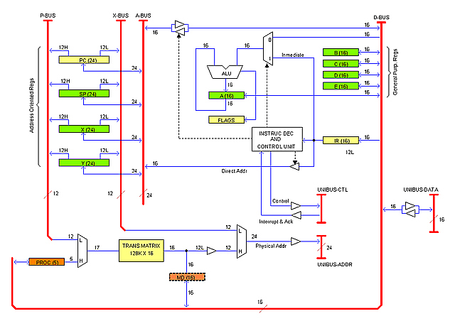
Today I could draw the first sketch of the CPU architecture or block diagram. It was surprisingly difficult; I expected to have a better idea on how to put together all of the ideas developed so far. But it was done any ways and it seems promising to me. By the way, I also came with a name for my computer: MDM-24 (stands for "Multi-Dimensional-Matrix" and 24 refers to the size of the Addr Bus). I like it because is similar to "PDP-11".
This is not actually the time for coming with a design, not even a block diagram. What is scheduled to do now is a specification. However, drawing the architecture for the first time got me a closer approach to implementation details that I feel useful to know in advance before writing the spec.
Anyways, what I drawn today is only a sketch that surely will change dramatically in the near future.
Here it is:
Resizing the Matrix
05/31/2009
Today I did two things: to read about mainframes and to play with different sizes for my Trans Matrix using a little utility that I improvised yesterday.
My readings were as in a tale of castles and prices. Now I realize why I don't like PCs: the real action is into mainframe engineering... but anyways, this is not about my professional frustrations.
As per the Matrix, it is almost decided that my computer will address words (16 bits), not bytes. Here are the results for different Matrix configurations:
-------------- CONFIGURATION # 1 -------------------------------------------
Max Memory : 32 MB
Page Frame size : 1 Kw (2KB)
Max simultaneous processes : 16
LINEAR ADDRESS: Width: 24 => Page field : 14 Offset field : 10
MATRIX ENTRY : Width: 20 => Control bits: 6 Physical Addr fld: 14
Matrix Size: 256K X 20 = 640 KB
-------------- CONFIGURATION # 2 -------------------------------------------
Max Memory : 8 MB
Page Frame size : 1 Kw (2KB)
Max simultaneous processes : 16
LINEAR ADDRESS: Width: 22 => Page field : 12 Offset field : 10
MATRIX ENTRY : Width: 16 => Control bits: 4 Physical Addr fld: 12
Matrix Size: 64K x 16 = 128 KB
-------------- CONFIGURATION # 3 -------------------------------------------
Max Memory : 4 MB
Page Frame size : 1 Kw (2KB)
Max simultaneous processes : 16
LINEAR ADDRESS: Width: 21 => Page field : 11 Offset field : 10
MATRIX ENTRY : Width: 16 => Control bits: 5 Physical Addr fld: 11
Matrix Size: 32K X 16 = 64 KB
-------------- CONFIGURATION # 4 -------------------------------------------
Max Memory : 2 MB
Page Frame size : 1 Kw (2KB)
Max simultaneous processes : 16
LINEAR ADDRESS: Width: 20 => Page field : 10 Offset field : 10
MATRIX ENTRY : Width: 16 => Control bits: 6 Physical Addr fld: 10
Matrix Size: 16K X 16 = 32 KB
----------------------------------------------------------------------------
This last seems close enough to reality.
Writing the Spec
06/01/2009
Research Phase is over. I am in the task of writing the Spec for hardware design. I am surprised that research have taken so short period of time. I think it was for two reasons: (1) I have devoted generous amount of time to it. (2) I left OS development matters for later.
In fact, my goal in this phase is to get specs for the hardware design (next phase). I finally could set the frontier between hardware support and OS job... that's helped. The hardware I'm picturing presents support for Multi-tasking and General Protection, and that's exactly what I needed for now, no more than that.
I also got the oficial name for my homebrew mini-computer: Heritage-1 (or "/1"; not sure if dash or forward slash). Heritage because... well, you know.
Research is over. Did I said that? Not quite... research never ends. I've done only the easy part. The real fun is yet to come.
Phase 2: Hardware Design
Decision-Making and Testing
My Spec is (intentionally) open so I'm now before a wide spectrum of decision-making challenges such as: What kind of components to use (TTL/CMOS, FPGA), going RISC or Microcode, whether to plan or not for Superscalar, Cache... that kind of things.
Obviously the only I can do is to tackle things one at time. Actually, each little part of the CPU circuitry (registers, ALU, Sequencer, etc) constitutes a whole World to me due my profound ignorance about these topics. It is truly difficult to make decision about things that you don't know well, but that has been my challenge since this project started.
Microcode or Hard-wired Logic?
06/03/2009
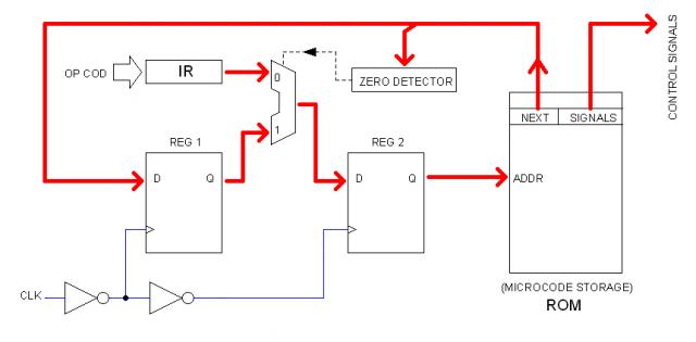
My first focus of attention has been the Instructions Decoder and Sequencer.
It seemed at first that Microcode is the only way to go. However, a quick research via Internet showed me that such decision is far from obvious, though very attractive indeed.
Microcode presents irresistible advantages to me:
- Easy to understand
- Easy to implement
- Naturally extensible
But it also has a disadvantage: It can get inefficient compared with other options such as a RISC-like hard-wired logic implementation, specially if one goes creative and build long, complex instructions. My computer will be slow for sure so I am almost obligated to compensate for that with efficiency.
Nevertheless I sketched a block diagram of what it would be my Microcoded Sequencer (I prefer to call it FSM since that's what it is basically). Here it is:
A brief explanation of the diagram is in here.
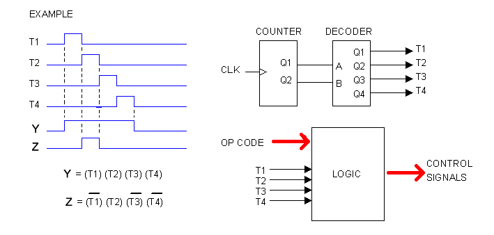
The other way is hard-wired Logic... which is not obvious either.
I had established that my op code is 16 bits. That is because my computer has the traditional Von Neumann architecture so data words and code words are the same width. I don't really know if there is sufficient room for field-oriented instruction encoding in 16 bits; that is something that I would need to explore.
Nevertheless I also asked my self how to decode without microcode and came with this approach:
For an explanation on how it works, click the link below:
index.php?branch=155
The fact of the matter is that I can't make a decision yet. Perhaps it is better to left this matter for later, when I had advanced the design of the CPU circuitry thus I had a better idea of what control signals I really need to produce.
Considering PLDs
06/03/2009
It is all about density. If I wanted to build a "pocket computer", I'd surely picked FPGAs. But I want my computer to be bulky, as in the old days. However, employing only SSI/MSI chips would make it "too bulky". That's why I'm turning to what is in between: PLDs, or actually a mix of PLD/SSI/MSI.
Moreover, FPGA portraits important constraints to me. To start with, I'm determined to use the traditional (and cheap) 0.100 inches prototyping boards, so I need all components to come in DIP packages. Adapter boards exist but they are prohibit to my budget.
Another problem that I see with FPGA is modularity. Being them so dense, I would be tempted to encapsulate large amount of logic in a single chip. Indeed I can always make changes to the firmware but that is not the kind of "modularity" I seek; it is not being able to start from scratch each time, but instead to be able to change one part without impacting others.
I started to explore PLDs today. ATMEL ATF22V10C, for instance, seems perfect for the "hard-wired" CPU Sequencer that I was picturing yesterday, no more, not less. I am thinking in those kinds of blocks and that kind of density.
The first step into reality
06/06/2009
From paper to the breadboard. Today the Heritage/1 putted the first leg on a tangible World. Like an embryo starting to take shape into the mother's belly, something like that. I'm very exiting.
Yes, I did the first breadboard test today. For details, follow this link:
index.php?branch=163
The test was really trivial but it gave me the necessary confidence. I have worked with logic circuits before; I have worked with microprocessors (8085, Z80) and Microcontrollers (PIC) as well. But building a computer without a microprocessor is totally new for me.
So today the project entered a new momentum in which I'll be designing and testing the building blocks of the Heritage/1: Registers, Multiplexers... From now on, everything is real.
Heritage/0 ?
06/11/2009
Early in the morning, a surprising idea came suddenly to my mind. A "pre-project": a computer prior the Heritage/1.
I was thinking that the things I need to test now (and before testing, design and build) are so very elementary that the overall prospective of a computer such as Heritage/1 is not actually needed. In other words, I don't need to test "the building blocks of the Heritage/1" but instead "the building blocks of a computer" (any).
And the surprising idea that came to my mind soddenly this morning was to put those blocks together to build a simple, very elementary computer. No Pages Tables, no "Matrix", no Supervisor Mode. No Operating System either (not now, no ever). Just the chance to peacefully concentrate in the very elementary building blocks that any computer of this kind needs to have, such as registers and buses, memory and interface with peripherals.
I think is a reasonable idea... I will consider it.
PREHER-816
Yes, I took the idea of putting the main project on hold to start this simpler "pre-project" called PREHER/816.
Designing the PREHER-816
Quick
06/12/2009
I won't spend too much time pre-designing without testing each little part, each little approach. That's why I need to buy prototyping boards and components sooner than it were planned for Heritage/1. So now I am in the terrible task of finding good prices specially for prototyping boards.
As per the chassis, I found a 3RU rackmout frame at a very good price ($180.00) in Digi-Key but I think I would prefer to build my own. It is because of availability. As Heritage/1, this computer is planned to be multi-units so I need to assure the existence of similar frames along years of development.
Rearranging the web site for PREHER-816
06/14/2009
Since I want to focus on PREHER/816 (now that Heritage/1 is on hold) I rearranged the site putting the old content aside in a book title "The Old Book".
Control Panel Lab
06/15/2009
Today I came with the (hopefully) final idea on how to build my hardwired Instruction Decoder and Sequencer (IDS). Details in here:
index.php?branch=216
But that is only the idea. Now it needs to be tested in practice and for that I need to design the actual circuit and build it.
I've been thinking all day about how to do testing in a regular basis. Unfortunately the breadboard is not too attractive to me. Simulators are not attractive either; they are slow and one have to spend time learning how to build phanton circuits with a mouse... not a "real thing".
The idea I came with is to build some kind of Control Panels with switches and LEDs that allows me to fill into the buses (using the switches), to read from them (LEDs) and to clock it (with a push button). This would be a permanent Lab device that also provides the regulated +5V for power and connects to circuits being tested via a ribbon cable. Something like that.
The idea is to have a "bus" that I can feed and read easily. With such a equipment it would be easier for me to build and test my circuits one by one.
Back to HERITAGE/1
Today (06/29/2009) I decided to make PREHER/816 the main subject of my project. The original "Heritage/1" idea is not longer "putted on hold" but postponed indefinitely so the current design will inherit her name. Why? Because (1) it is an appropriate name, (2) because working on a "pre-project" is quite frustrating and (3) because I wanted to stop the mess of names once an so ever.
So from today on "Heritage/1" refers to the machine I am making now, which is the main and the only one.
BUS LAB
06/29/2009
Before going further, I will build this development tool that I need to test circuits as they come. It is basically a manual signals generator and monitoring tool that will provide control signals (Switches) and will monitor buses status (LEDs). More info in here:
index.php?branch=228
Buying parts for the first time
06/28/2009
Today I ordered parts for the first time in the history of this project. They were 10 prototyping boards from Jameco and some nice (and cheap) switches from Gold Mine Electronics.
I am specially happy with the proto boards because it have been difficult to find good sizes at good prices. This is not particularly cheap (5.5 x 8 inches at $10.95) but is the best I could get and it's not bad at all.
The switches look really nice in the catalog (I hope they are as good) and the price couldn't be better: 59 cents each... I ordered 100 at once!.
The BUS LAB is not designed yet but I need the switches with me before I can make final design decisions. Since switches and other parts need to fit in a panel, physical dimensions count more than one can imagine.
16 Bits: A shine of elegance
06/30/2009
I seemed happy enough with my 8-bit design when suddenly, at mid night, a totally different design came to my mind and I had no option but to jump to my acrylic white board and start sketching the new idea. I don't want to post anything yet other than this little note, until the idea is more mature.
The new architecture for the Heritage/1 is 16-bits both address and data. This means that all registers are 16 bits and implies that any of them can be used as a pointer. This simple fact completely defeats the notion of "data-oriented" and "address-oriented" registers.
Indeed this is nothing new. The PDP-11 was just like that and same approach has been followed by homebrew CPU designers like John Doran.
As per my Heritage/1, I have the following plan:
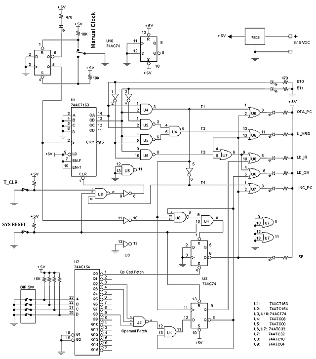
Except for special registers such as IR (Instruction Register) and MDAR (Operand holder), all regs will be built using counters (74HC169). This allows the CPU to execute INC/DEC instructions in just one clock cycle since no ALU operation nor data transfer is involved.
Not only counters, of course, but 3-state buffers (74HC244) too. Actually, each reg will have two buffers: One to the internal D-BUS (Data Bus) and the other to the external Address Bus. This way each reg can write to either bus. Inputs, however, always come from the D-BUS.
The other change has to do with the instruction decoding mechanism. I'm still determined to use hardwired logic instead of micro-coding (that is for the sake of speed and also because I find it more interesting); however, now that I have a 16-bits instruction (instead of 8) I have room for field-mapping.
This is the idea:
No matter what the data transfer, there are always two registers involved: a source (SRC) and a destination (DES). If data is transferring between registers, that is pretty clear; if it is from or to memory, one register is receiving or sending the data while the other is supplying the address (Ex: PC, SP or any reg used as pointer in a indirect addressing instruction).
So for any data-transfer instruction I only need two fields to say what registers are involved: SRC and DES. For the current design, 3 bits each would be enough, but I will make them 4-bits so I have room for 8 more registers in the future.
After had expending 8 bits in field-mapping, I yet have 8 bits for instruction OP-COD so I can build up to 256 instruction which is more than enough.
And having this reg addresses coded within the instruction I can simplify the logic by using 4-to-16 decoder chips. I will use three of them: One for "data-read" (open buffer to D-BUS) control signals, one for "data-write" (clock registers) control signals, and the other for "address-open" (open buffer to the Address Bus) control lines.
That is basically the idea for the new architecture. I think is elegant and promising. And I hope not to come with a new redesign before this project evolve in a total mess.
Buses, Cards and Backplane
07/06/2009
The problem I have with the BUS LAB is with connectors: not clear on what kind of connectors to use. This concern took me to the CPU buses and connectors but in this case it was different: I could make final decisions about my buses both internal and external, the backplane connectors to use (DIN 96-PINS) and I also could get some idea of how many Cards the CPU might take (about 8).
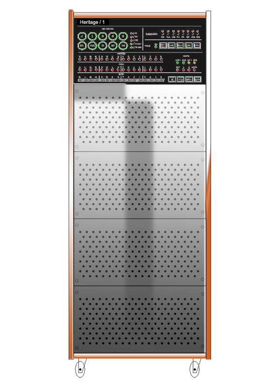
I pictured my cabinet too: a refrigerator-like enclosure, tall and bulky as most minicomputers on the 70's. Now I can imagine the Heritage/1's "body", not just her "spirit"...
As per the BUS LAB, I haven't designed it yet.
Approaching a final design of the Internal Bus
07/07/2009
Looking for standards I got to the VME Bus P1 which utilizes the same 96-PINs connector I chosen. This bus is designed for computers and it designates many power and control lines that I don't need for my Internal Bus, but I decided to adopt the pin out discarding those signals that I don't use but retaining those that I do; these are: 16 Data pins, 16 Address pins, SYS CLK, 8 GND pins and 3 +5V pins. Discounting the rest out, I have 53 extra pins for anything else.
I started wondering if that would be enough for my control signals, that is if my previous forecast of about 70 were currect. In order to approach the answer, I did a detailed signals count over the CPU block diagram. The final pin-count surprised me: only 46.
Of course, in practice they will be more and there will also point-to-point connections between certain cards. But it still makes sense to consider the 53 extra pins for a possible "control signals bus".
Taking shape
07/09/2009
Heritage/1 starts to take shape. I have a very clear idea about the Buses both internal and external, and specially how to build the CPU backplane, how to connect it to the External Bus and to the Control Panel... yes, I also know how the control panel it's going to be and where will be within the circuitry.
And finally, I also have an idea about how I want Heritage/1 to looks: like a refrigetator, as most computers were in the past. Here is a very first look to the Heritage/1 "body":
Opsss... Pins count exceeds the limit
07/17/2009
Today I made a quick approximate count of all control lines needed and it gave me about 65 which is more than the 57 currently available in the C-BUS.
So far the CPU Backplane layout, internal buses, distribution of resources among cards and similar details are well defined, so I can have much better idea of how the CPU will be and how many control lines it will need at the end. The only problem is with my pick of 96-pin connectors for the Backplane.
Actually, the problem is caused by the need of a Control Bus (C-BUS) consuming all control lines so all control pins at once for all controller cards. The need for a bus comes in turn from the existence of more that one IDS card controlling same control lines.
CONCLUSION: I have no choice but replacing the 96-pin connector with a big one. I have to examine this later with more detail, but the solution seems to be in to keep using 96-pin connectors (DIN 41612 Type C) for Data Slots but for Control Slots, use 160-pins connectors (DIN 42612 Type C Extended) instead.
Since nothing have been built yet, that is not big deal except for the cost increase.
First Schematic finished
7/18/2009
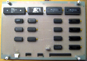
Today I finished the first "official" drawing: the H1-REG1-1 card schematic which contains the main registers of the computer: PC, SP and the Operand Register (OR). The circuit is composed by 23 chips fitting comfortably in my 5.5x8 inches prototyping board. The drawing took three sheet of paper (I am drawing for letter size: 8.5x11 inches).
I am very happy because this can be seen as the first step into reality: something that can be built and tested. I plan to start doing just that very soon.
First board being built
07/19/2009
Today I started building the H1-REG1-1 card. It includes registers PC, SP and OR. My plan is to build the first register first (PC) and start testing before building the other two.
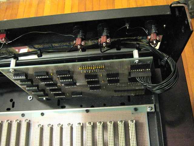
In order to be able of doing testing, I also assembled a Backplane: just connectors soldered to a PC Board and buses wired in the back. This setup is all I have for now for start testing the most elementary circuits in my computer: registers.
New in town: The Fetch Sequencer
7/23/2009
For the last few days I was having a really bad time trying to figure out the way of "decoding" an op. cod. fetch cycle. My original idea was to use the condition IR=0 (no op code) to trigger the OP COD FETCH sequence, but I'd always conceived this sequence being generated in the IDS card, hence the problem.
The thing is that reading the OP COD directly into IR (this takes place during T3) breaks the sequence right there, just when IR stops been zero. The obvious solution is not to read the op code directly into IR, but I cannot afford it because that is precisely the core of the Heritage/1 philosophy: to read things directly where they go in order to minimize data transfers... moreover, to eliminate intermediate data transfers at all.
Fortunately I found another solution. My original idea holds: The condition IR=0 triggers the OP COD FETCH sequence, but the circuit providing the sequence is not in the IDS card but in the MASTER CONTROLLER CARD. I called this circuit: "Fetch Sequencer" and it's relatively simple.
One curious detail about which I'm not entirely sure yet: This circuit will also generate the sequence for the Operand Fetch cycle. I mean, if the instruction requires operand fetching, the sequence will continue taking clock cycles T4, T5 and T6 to read the operand from memory into register OR. Then it will reset the T-COUNTER and deactivate the SF signal so IDS cards can take control... Is this... "natural"? Not sure, but I think it works... on paper at least.
Instruction Set Architecture
7/25/2009
Today is Saturday and I went no where. Instead, I spend all day defining the final Instruction Set Architecture up to the ultimate details.
I came with the concept of "Instruction Classes" to group instructions that are similar in implementation so I can reuse decoder circuitry. I also defined all instructions in my Set and all ALU operations (they are not too many).
Curiously, the design taken me to unexpected results such as the "multiple" INC/DEC instructions (Ex: INCM E, D) which "naturally" increment two registers simultaneously in a single clock cycle. This is the kind of surprise that I really enjoy.
Honesly, it has been hard for me to get to this point. Decoding instructions with hardwired logic resulted more difficult than expected, specially since that logic must be distributed among several cards. The Heritage/1 experience has been unique in that regard: the first circuits drafted were unacceptably complex but they were gradually gained in simplicity up to what they are now: unbelievable simple circuits.
The core of Heritage/1 design is still simplicity, which ironically contradicts the very nature of a (complex) project of this kind.
Bus Controller and the new Backplane
7/29/2009
The idea of adopting the VME bus (with modifications) never convinced me entirely although I've had accepted it as a fact. Two thing bothered me: The large amount of ground pins and the fact that I was adopting a standard used in a non-standard way. Besides, what is the need? I don't plan to plug factory-made VME cards in the Heritage/1 nor to place Heritage/1 cards in a VME bus, so the adoption didn't seems very useful.
Yesterday, I decided to put an end to the insanity by making my own proprietary backplane. It is divided into two halves: Data Slots and Control Slots, as planned before. Data slots use 96-PINs DIN 41612 connectors. Control Slots use 120-PIN DIN 41612 connectors. I had the former since last week; the later was ordered today to Digi-Key.
Another important decision I made today was about the BUS CONTROLLER Card. This is a card interfacing both Data and Control slots. The problem I had with this card had to do with connectors; I simply don't want my cards (any card) to connect in any way but through the Backplane... I hate the idea of having ribbon cables coming from one card to the other taking "unofficial" paths.
I had imagined the Bus Controller as a double-card so it could have two connectors: one 96-PIN plugging in a Data Slot and one 120-PIN plugging in a Control Slot... but that never got to convinced me. The definite solution came suddenly while I was at work: a larger card with the two connectors in-line. This card will not be placed vertically aligned with the others but horizontally below (or behind). Problem is that the cards I have now (5.5x8 inches) are two small for two connectors. So what I did today was to order five larger cards: 9x6 inches. These cards will also be used for building the Backplane itself. And this gave me a much better idea of how the CPU frame will looks like.
I am very happy with all this, only that the cost is increasing. So far I have expended little more that $600... just in switches, connectors and prototyping boards!
Parts are on their way
7/31/2009
This month of July has been very active for the Heritage/1 project. It has been the month in which the design has taken its definite shape. However, everything is still on paper.
The month finishes with 740.44 dollars in expenses. Next week I'll be receiving the necessary chips, ic sockets, diodes, caps and other components for start testing what is on paper now.
Breadboard testing
During this phase I will be doing design and testing, one part at the time, in the form of separate experimental circuits.
Fetch Sequencer
08/11/2009
Today I finished building this little experimental circuit and started to test. The experiment revealed some design problems but it started to work as expected after minor changes were made.
This is the first test of a "sequencer". The technique tested here will also be used for decoding instructions in IDS cards. Here is the schematic for the working test circuit:
Introducing the L-BUS
8/20/2009
Today I introduced a new CPU internal bus named: L-BUS (Lamps Bus). This 24 lines bus will be present in Data Slots specially for registers.
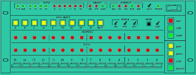
Registers will write to the L-BUS so its content can be displayed in dedicated LEDs on the Console. At a given time only the selected register writes to the bus (selection comes from the Console). The first 16 lines (L0-15) are for register's content whereas L16-21 show the current status of the register's control signals: CLR, LD, INC, DEC, OTD, OTA. Lines L22 and L23 are wired but not used and always read "inactive" (wired to +5V since all control signals are active low).
Now registers feature a third output buffer (in addition to the two they already had) and a new input control signal named: OTL (Output to Lamps) which selects the register to be shown.
This simple idea have brought three consequences to me:
1.- Registers are now bigger (and more expensive), not very easy to fit more than three of them in a card of 5.5x8 inches.
2.- I can not longer draw for letter-size sheets but for 11x17 inches instead.
3.- The way for the Console's operator to read register's content is now a lot easier.
To be honest I had opposed to this idea until now. That is because I wanted to restrict the Operation to the CPU architecture, that is: if one wanted to see a register content, then he or she needed to open that register to the internal D-BUS (switch OTD, Open to Data Bus).
However, when I started designing the Console's control circuitry, I found that the interconnection between this card and the Master Controller Card were taking too many pins. I found other problems related to selection logic so I decided to "distribute" the selection among register cards, hence the L-BUS.
The Operator (... what operator apart from my self?) will be happy with the new design since now he will be able to watch any register content (as well as their control signals) very easily by just selecting it... not sure if by mean of push buttons or a rotary key.
Introducing the Arbiter Circuit
08/23/2009
Until now, control coordination between the Fetch Sequencer, the IDS cards and the Interrupt Controller relied on four "status signals" (SH, SF, SE, SI: Status Halt, Fetch, Execute and Interrupt respectively).
Problems arose when I started to sketch the actual circuits. These signals came from different places to fight each others under inhibit/enable rules. At the implementation level, that proven to be a mess.
I came today with a different, much more decent approach. Now the status is coded in two signals named: S0 and S1, according with the following table:
S1 S0 Status
- - - - - - - - - - - - - - - - - - - - - -
0 0 Halt
0 1 Fetch (either code or operand)
1 0 Execute
1 1 Interrupt being negotiated
These signals comes from a new circuit called ARBITRER. IDS cards and the Interrupt Controller listen to them and keep themselves inhibited until the appropriate status arrives.
When execution finishes, the IDS generate an "End Of Execution" (EOE) signal back to the ARBITER which in turn generates the appropriate signals to either halt the computer (case of STEP execution) or clear the IR to enforce the new Fetch cycle. Similarly, the Interrupt Controller rises an "End of Interrupt" (EOI) when negotiation with peripheral is over.
Small Cards: a challenge
08/26/2009
The challenge that using small prototyping cards represents is becoming more and more apparent.
For one part, register circuits have grown during the last week. Recently, the L-BUS was introduced and now I'm wondering how I'm going to raise flags and even detect fault conditions from the registers themselves. That will be by adding more chips, obviously. Will them fit?
In the other hand is the connector pin-count issue. I have designated 70 of the 96 pin available at Data Slots so only 26 are left for point-to-point control signals. My "standard signals" add 6 per register so the pin-count by itself limits my cards to have 4 registers at the most with only 2 pins left for additional signals.
That still matches my original plan (PC, SP, OR in one card; B, C, D, E in another card and A in the ALU card) but feeling as being pushed to the limits is not nice.
As per Control Slots (120 pins), 37 pins are designated already, 83 are available. A comprehensive count of register's control signals resulted in 55 total so there are still 28 pins available.
Not all of these remaining 28 pins can be connected in a bus (as the others are) because I will need a few of them (about 8) for point-to-point connections. For instance, the "End Of Interrupt" (EOI) signal coming from the Interrupt Controller.
I wouldn't like to make more significant changes to the design so for now I will keep going on with this tight situation.
Control Panel Layout
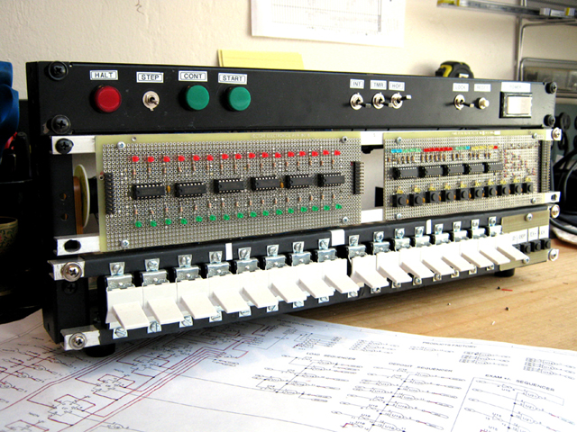
8/28/2009
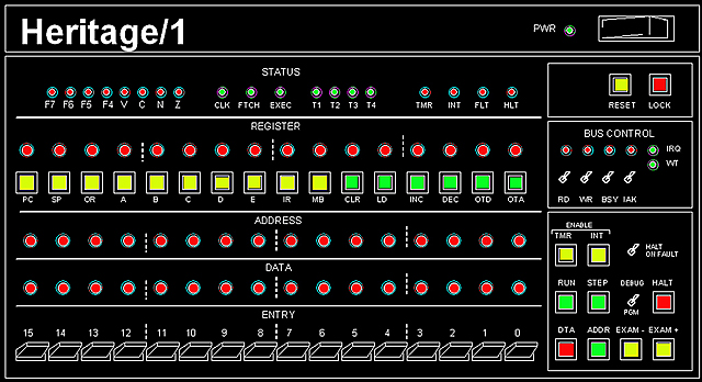
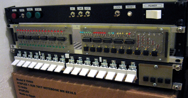
I'm kind of stocked with the Arbitrator and the commands comming from the Control Panel, but I hope to solve that soon. The Control Panel (or Console, as I also call it some times), is almost definetely decided. It will look more at less like this:
The illuminated square buttons cost about $15 each so not sure if I will use exactly those.
Memory Bank register: defeated!
A few days ago, I submitted the project to comprehensive revision under severe criticism. I wanted to make sure that all the ideas developed so far were strong enough. Most of them hold; some (such the Interrupt Architecture) resisted not without difficulties. The only one that did not pass was the use of Memory Banks (register MB).
This technique seeks two purposes: (1) To expand the "limited" 64K words memory address space, and (2) to provide a rudimentary hardware support for General Protection in the future. Neither of these arguments proved strong enough; here is why.
The 64K words limit
From the "historical" point of view, 64K words matches the old-fashioned technology being employed. Most minis in the 60s and 70s came equipped with about 8K words, being 64K a costly luxury. It was using one of those minis (DEC DPD-11) that the UNIX operating system was invented.
From a realistic viewpoint, I'll be writing software in plain Assembly language for a long time. Even when I could envision the developing (or porting) of a full featured operating system in the far future, it is hard to imagine the need for more that 64K words of memory due the kind of software that Heritage/1 will be able to run in practice.
Lets imagine, however, that 64K proved limited at some point in the future. In that case, I will be happy then to accept the challenge to start developing solutions both in software and hardware.
Rudimentary support for General Protection
Years will pass before I embark into Protected OS development and chances are for so to never happen at all. Hence the weakness of providing such a support from the very beginning. Besides, I cannot tell if memory banks (allocating different processes in different banks) will actually work.
Conclusion
The removing of the MB from the architecture honors the original idea of having data and address the same size. Software will get simplified by not having to declare the current memory bank. Circuitry will also gain in simplicity.
As per the subjective side of the project, I now feel better to have a decent provision of memory that matches the historicity of the machine being built.
The only thing that is still bodering me is the use of modern SRAM memory chips. That, however, will be very hard to "fix".
Introducing Relative Branches
09/22/2009
Last night I was thinking on how an Operating System (even the most rudimentary one) would manage to allocate programs in memory from Storage. I realized that those programs must be written using relative addresses instead of fixed ones. That could be done using the already provided "indirect branch" instructions (such as "JNZX reg"), but the correct way is to implement actual "relative branch" instructions.
For implementing this new addressing mode, some modifications need to be made. Fortunate the modification in question is quite simple and, after all, the computer is still on paper (nothing has been built yet) so this is the time.
The new addressing mode (relative) will only apply to branches because extending the concept to all registers would lead to profound changes to the overall architecture. I don't want that.
An example of relative branch instruction is this:
jnzr OFF_SET
where OFF_SET is an operand to be fetched from memory (following the op code). Executing this instruction will cause the Program Counter to add OFF_SET to its current content so the next op code fetch takes place OFF_SET memory locations further.
This will allow an OS to allocate programs anywhere in memory since those programs won't care about where they are but only how far they need to jump.
Arbiter circuit tested
10/3/2009
Today I tested this simple Arbiter circuit, which proved correct.
The circuit was built in a prototyping board and tested using simulated signals coming from debounced switches. Output signals S0, S1 was displayed using buffered LEDs.
Principle of Operation
The circuit is actually a Finite State Machine (FSM) implemented with two D-type flip-flops (74ATC74) which outputs represent the status signals S0, S1. A simple combinational logic takes those, combined with others, and feeds the data (D) flip-flop's inputs with the "next status". The FSM changes status when the flip-flops are clocked by a "stimulus" signal provided by a logical OR of all possible "stimulus signals": /EOF, /EOE, /EOI, /START. (Note: In the diagram, the "logical OR" is actually a logical AND (U1) because input signals are active low).
The /START signal is a "pulse" provided by the Control Panel circuit. It occurs when the Operator pressed either HALT, RUN or STEP button on the Console.
The status output signals S0, S1 represent the current status of the computer, according to the following table.
S1 S0 Status
- - - - - - - - - - - - - - - - - - - - - - - - - -
0 0 Halt
0 1 Fetch Cycle
1 0 Execute Cycle
1 1 Interrupt being negotiated with peripheral
- - - - - - - - - - - - - - - - - - - - - - - - - -
Different circuits (such as the Fetch Sequencer, the IDS cards and the Interrupt Controller) use those as enable/disable signals. For instance, the Fetch Sequencer inhibit itself when S1,S0 is different from 0,1.
After reset, the Arbiter is in Halt status (S1,S0 = 00). When the operator pushes the RUN button on the Control Panel, the Halt flip-flop gets reset (/HLT=1) and the Arbiter changes status to S1,S0 = 01 to allow the Fetch Sequencer to start a new Fetch cycle.
Once the Fetch is completed, the Fetch Sequencer rises an "End of Fetch" (/EOF) signal which forces the Arbiter to change status to S1,S0 = 10; this authorizes IDS cards to start the Exec cycle.
When the Exec cycle finishes, the IDS card rises an "End of Execute" (/EOE) signal, signaling the Arbiter to change status again. The Arbiter decides what next according to the following logic:
If the Halt flip-flop is reset (/HTL=1) and there is not a pending interrupt request (/IRQ) from the Interrupt Controller, then:
- - - - - - - - - - - - - - - - -
Current --> Next
- - - - - - - - - - - - - - - - -
0 0 --> 0 1 Go Fetch
0 1 --> 1 0 Go Exec
1 0 --> 0 1 Go Fetch
1 1 --> 0 1 Go Fetch
- - - - - - - - - - - - - - - - -
If the Halt flip-flop is set (/HLT=0), the output is forced to S1,S0 = 00.
If there is a pending IRQ, the output is forced to S1,S0 = 11 which authorizes the Interrupt Controller to start the Interrupt Sequence (negotiation with the interrupted device). When the sequence finishes, the Interrupt Controller drops the /IRQ signal and rises an "End of Interrupt" (/EOI) signal; in response, the Arbiter change status to 01 (Fetch).
Neither /IRQ nor /HLT signals will be sensed until the last execute cycle has finished, that is, when /EOE is active. This ensures that no instruction cycle will be left behind in the middle of the battle.
The Heritage/1 LAB implementation
During this phase, a LAB implementation of Heritage/1 will be built. The final machine will be built much later, after the "LAB" has became mature and fully functional. Most parts from the LAB will be reused to build the final machine.
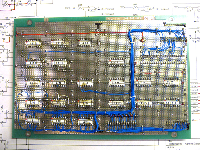
Wiring the Backplane
10/10/2009
I started to wire the backplane consisting of 6 "Data Slots" (96 pins), 6 "Control Slots" (120 pins) and one "interconnection slot". I've seen that this is quite a slow task since it took me 10 minutes to wire just one of the numerous bus lines. Nevertheless I plan to have the Backplane wired by 10/24/2009.
What about "micro-dioded" logic?
10/12/2009
Considering the use of small diodes matrixes. See discussion in the BrainStorm book:
http://www.armandoacosta.com/cpu/index.php?branch=390
Entry Swithes: just another register
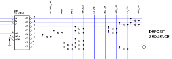
10/19/2009
Here is a simple idea, so simple that I still wonder why it didn't occur to me before: The Entry Switches are nothing but another register within the CPU.
For "normal" registers, I have a set of lamps and buttons on the Console to select one register at the time, show its content as well as it's control signals status and also to CLEAR, LOAD, INC, DEC and open its buffers to either the internal Data Bus or the Address Bus. Well, if Entry Switches are another register, then it must be present in that buttons/lamps set.
Thus, I will simply add another button labeled "SW"... (in place of the "MB" wich is not longer needed).
By pressing that button, the operator selects the Entry Switches for watching its content in the lamps. He also will be able to dump its content to the Data Bus (button "OTD") or to the Address Bus (OTA) as with any other register.
For example, if I want to load the IR register from the Entry Switches, I press the "SW" button, enter the desired content in the switches, then I press the "OTD" button so the content is available to the internal Data Bus; then I select the IR register by pressing the "IR" button and then press the "LD" button to load that register from the Data Bus.
That is when the computer is in "Debug Mode". In "Programming Mode", the Entry Switches behavior will be totally different. In Programming Mode, the operator needs to be able to examine and/or alter memory content and to run a program starting in a given (by switches) memory address. But that is an old story, I mean, I had conceived that part before.
Two boards for one Console
10/26/2009
I haven't find a clean, elegant solution to the problem I had with the Console, until now (a few minutes ago). The problem is this:
The Console is a "controller", actually the "ultimate resource" when things go wrong with the computer circuitry. But the Console is not just a bunch of lamps and switches but logic as well so it takes board space (more than I expected) and, what is worse, it takes a lot of pins.
I were conceiving a "Console Board" to allocate such logic, but this board would not attach to the Backplane but to the "Master Controller Card" which in turn plugs to two slots (Data and Control) being the only card in the CPU with such a privilege. The Console needs signals from both Data and Control slots hence the need for been connected to the Master Controller Card.
This arrangement never pleased me but no better idea had came to my mind. The worst part is the large amount of interconnections between the Master Controller and the "Console Board", made with ribbon cables plugged to header connectors (something that I truly heat!)... By the way, all this is still on paper, nothing has been built yet.
And, yes, fortune smiled to me just a few minutes ago when I came with a different approach which is this: No one but two Console boards.
One is called the "Console Monitor Board" and it plugs to a Data Slot just as Registers cards do. This cards is responsible for collecting and buffering data from the buses (D-BUS, A-BUS and "Lamps Bus") just to be presented on the Console's lamps (LEDs). It also contains the Entry Switches Register.
The other card is called the "Console Controller Board" and plugs to a Control Slot just as other controllers (such as IDS and the Interrupt Controller) do. It contains the Console's logic and rises internal control signals in the same fashion other controllers do.
So there is nothing special with "console boards"; they are regular "data" and "controller" cards and they follow exactly the same rules. This solution will simplify wiring and will allows me to allocated the different Console's circuits in a comfortable manner.
I think this solution is elegant, but what makes me really happy is to see how the overal design is guiding my mind to every specific solution in a natural way, so it makes me to conclude that the design is, indeed, an elegant one.
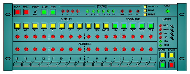
Removing sixteen LEDs from the Console!
10/31/2009
While sketching the Entry Switches registers, I realized that I don't really need dedicated LEDs for monitoring the internal DATA BUS. In fact, the L-BUS allows the operator to select whatever he wants to watch so I can simply let him select the DATA BUS as well, in the same way he selects any other register.
What I had named "REGISTER" (LEDs) now becomes the "DATA" LEDs. And what I'd named "DATA" (LEDs), simply disappear.
As per Entry Switches, I don't need to latch them during Debug Mode. The operator can treat the Entry Switches as any other register only that a manual change in the switches themselves will be reflected immediately.
For Programming Mode, I will introduce two specialized registers called "Programming Data Register" (PDR) and "Programming Address Register" (PAR). These registers will be used by sequencer circuitry located at the Console Controller Card for performing the memory data read/write cycles required during Programming Mode.
|
This new arrangement not only simplifies wiring (16 less connections!) but it also fits better within the overall design.
Three registers will not fit in a single card
11/04/2009
Registers have gone too big, specially with the addition of logic for detecting Conditional Status. A typical register such as B, takes 14 chips plus additional logic so the three registers per card that I've planned would take more than 42 chips which definitely don't fit in a 8x5.5 inches prototyping card.
I have two options: (1) To use larger prototyping boards, (2) to distribute registers in a different way (2 regs per board at the most). The former is too expensive; the right card costs almost twice (about $20.00 from Digi-Key) that my 8x5.5 inches boards. Hence I'll take the second choice.
Here is the new distribution:
Card Name Registers
- - - - - - - - - - - - - - - - - - -
H1-REG1-1 PC, OR
H1-REG2-1 SP
H1-REG3-1 B, C
H1-REG4-1 D, E
H1-ALU-1 A (and the ALU)
Concern with the idea of having a "Control Bus"
11/10/2009
For more than four months the design has kept stable based on certain "primary ideas" that have hold so far. One of those ideas is to wire all control signals together in a bus in "Control Slots" so all Controllers have access to those at the same time. This allows me to have more than one IDS (Instruction Decoder and Sequencer) card, which is good because it represents modularity which is convenient.
There is a price to pay, however: the increase of pin-count. I was been forced to purchase expensive 120-pins connectors for "Control Slots" just because of that. And not just money; another problem is with the Console, which takes many interconnections, that is many ribbon cables plugging to header connectors anywhere within the computer, which is a mess.
That's why I am revising the "primary idea" of the "Control Bus" in the sake of solutions. I wish to have all conations through the Backplane only: not a single ribbon cable plugged to any card at all. The only way I could get to that is by removing pin assignments from the Backplane connectors. The obvious opportunity is with the Control Bus.
I realized that the only cards that really need access to all control signals are the IDS cards. Other controllers such as the Interrupt Controller and the Console Controller only deal with a few control signals. Therefore there is no need (other than simplicity) to wire all 75 control signals to all Control Slots; it is sufficient to wire them to IDS slots. This would free a lot of pins for the Console Controller that could be used to connect to the Console.
The bottom line is to defeat the simple idea of having just two types of Slots (Data and Control). The new approach would be to wire the Backplane more efficiently putting wires where is really needed.
Honestly, I'm not entirely happy with this approach because it will prevent the mess of ribbon cables at the expense of creating a mess in the Backplane wiring. So I'm not making a final decision yet, but just researching the matter very carefully.
The fall of two milestones
11/21/2009
Last week was busy in terms of crucial decision making. If Heritage/1 were a real machine being designed by a real-world manufacturer, last week were be one of hot meetings and heavy memos.
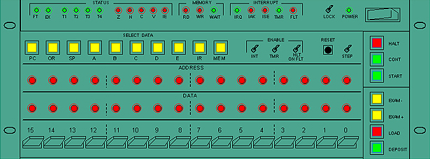
Two milestones was definitely defeated: The division of the Backplane in DATA and CONTROL slot types, and the old idea that the Console must offer static hardware debug capabilities.
The former opens an important opportunity: the possibility of wiring the Console's panels directly to the Backplane via ribbon cables ended with header connectors. So far I simply had no pins left in the Backplane connectors for that so ribbon cables had to connect to a card which is not a clean solution.
The later resolves a tremendous bottleneck that I had with the Console's design since "debug capabilities" turned very complex in implementation. Its removal has lead to accelerate the project in a notable manner. Here is the new Console without hardware debug capabilites:
The Ruch for the Backplane
12/01/2009
I'm moving to produce a Backplane as quick as possible. Having the Backplane and the Console (not only the actual panels but also the boards that provide its functionality) I will be able to move the project into �scalade mode�, that is building the machine board after board.
That's why I am a real ruch to finalize designs for both the Backplane and the Console. They are actually, pretty much, finished so I'm making preparations for ordering the necessarry parts.
Console boards being built
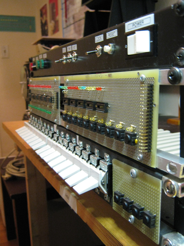
01/26/2010
Panel circuits design is complete. It took four boards: two for push-buttons, LEDs and buffers, one for console registers and one for console functionality. The first board was built and the second well be finished soon.
Micro-dioded logic discarded
2/5/2010
I've been considering the use of diodes matrixes for a while, or what I called "micro-dioded logic". However, a simple "test of concept" experiment proved that the use of a diodes matrix for building sequences is not a good trend.
The images below shows a portion of the drawing. You can see the matrix rows being fed from the Decoder's outputs.
As expected (hence the purpose of the test), sparks appear at those points when the decoder's outputs change.
I could cut the spark with a simple RC low-pass filter circuit (R=100 Ohm, C=47pf), as shown bellow:
However, this is not the kind of solution I seek, so I decided to discard Diodes Matrix all together as a technique for building sequences.
Manuals
02/10/2010
Rearrenged the site to accomodate the Heritage/1 Manuals: Operator's Manual, Engineer's Manual and Programmer's Manual. The idea is to filter out old irrelevant content for having clear ordered up-to-date information into these books.
Two months of inactivity
04/09/2010
This project has been "frozen" for two months as I turned to other priorities that I have in life (including my work). Currently, my free time is still scarce but nevertheless I decided to retake the project in the aim of getting to the "escalade phase" as soon as possible.
I started by reviewing notes and schematics to proudly found that the project is in very good shape: implementation ideas and solutions are mature (stable) so I can continue by the exact point in which the project was left two months ago.
The focus now is into producing the Console and the CPU Backplane as those are the infrastructure required by the "escalade phase". The bad thing about it is that it will take long (about four months) and, because separate testing is not too feasible, all of those parts will possible be tested at once, hence to make them to really work will take even longer. I don't expect any thing truly functional before the end of this year.
Building the Console Controller
05/05/2010
I'm currently building a board named: "Console Controller". It produces the sequences to carry out the Console commands: LOAD, DEPOSIT, EXAMINE- and EXAMINE+. It also handles other Console functions such as "Panel Lock".
This is important to the project as it will serve to prove two concepts: (1) The technique being employed for producing sequences by hardwired logic (see Building sequences with combinatorial logic) and (2) the construction technique being employed to actually wire boards by soldering (see Why are you soldering instead of wire-wrapping?).
So far, so good. The wiring process is quite slow but it is easy to make changes when needed. I do the wiring in two steps:
Step#1: I "prepare" the board by placing components and connectors, wiring power pins with naked wires and placing naked "half-moons" that will serve to guide signal wires is step 2.
Step#2: I patiently start connecting the signal wires using the "half-moons" as physical guides. Partial tests are performed during this step.
If I had a lot of time, building a board that way would take about a week. Unfortunately that is not the case so it is taking a little longer...
Writting the Heritage/1 Assembler
5/31/2010
Started to write an Assembler for Heritage/1, called H1ASM v.0.
I had no plans for start building my development tools yet. Moreover I was aimed to purchase a commercial cross assembler or to seek an open source one in the Internet. However, I started to think on how could I write one that is very simple. Soon I realized that it may be not too hard if I content my self with writing something really, really simple.
I started by cutting the Linker at once, that is my assembler will act as a "stand-alone" guy capable of directly generate the executable code. This leads to serious limitations indeed but it also simplifies tremendously the assembler on its own.
Macros were also discarted as well as conditional compilation and other "advanced" features that real assembler ususally offer. My assembler will be so simple that I'm not longer scared by the task of writing it entirely from scratch.
I chosen PHP command-line interface (cli) because it is easier than C, as code doesn't need to be compiled. Moreover, being PHP a popular scripting language, my assembler will be able to run on Linux, Windows or Mac OS-X and even ported for a web environment with little effort.
I started building the code up the point that I have a comfortable infrastructure. But now I'm more concern with the production of the Programmer's Manual, which is actually my SPEC for guiding my self during the development cycle.
The (unfinished) Manual is already published in this site, here is the link:
http://www.armandoacosta.com/cpu/index.php?branch=533
Reducing the Fetch cycle to 3 periods instead of 4
6/1/2010
Tonight, an old premise (held since July 2009) fall, resulting in a 25% increase of the average performance... according to raw calculations.
It was established since before that the Op. Code Fetch cycle should take 4 clock periods:
T1 Open PC to the A-BUS (OTA_PC)
T2 Memory Read signal (MRD)
T3 Read the bus into IR (LD_IR)
T4 Increment PC (INC_PC)
Since every instructions requires an Op. Code Fetch cycle, this T4 doing nothing else apart for incrementing the PC represented a serious waste of overall execution time. Here is how I took it away.
Following the Op. Code Fetch cycle is either the Operand Fetch cycle or the first period (T1) of the exec cycle.
I realized that PC is never used in execution during T1. Even branch instructions (the only ones that get to write into PC) don't touch that register until T2, so we are really plenty of time during T1 for activating the INC_PC signal in order to increment PC at that time. This will reduce the Op. Code Fetch cycle (as well as the Operand Fetch cycle) to 3 periods instead of 4.
So now we have:
---- Op. Code Fetch ---------------
T1 Open PC to the A-BUS (OTA_PC)
T2 Memory Read signal (MRD)
T3 Read the bus into IR (LD_IR)
--- Exec --------------------------
T1 Increment PC (INC_PC)... apart from whatever the instruction needs to do.
T2 ... the instruction continues to execute.
Doing the same for Operand Fetch cycle is also possible. PC was opened to the A-BUS during Op. Code Fetch and now it needs to remain open during Operand Fetch while it's being incremented (at T1); however the Memory Read signal (MRD) will not come until T2 (250 ns later) which is long enough for the data to stabilize in the bus... (I hope).
An additional advantage is that now the INC_PC signal can be obtained very easily. In fact, INC_PC must appear always at the same time: T1 of either Operand Fetch or Execution cycles.
The machine "knows" that she is in Exec cycle because S0=1 and S1=0. It also knows of T1 because ET0=ET1=0. Decoding such condition will be enough for obtaining the INC_PC signal. The Fetch Sequencer circuits will need to help, however, by providing INC_PC during T1 of the Operand Fetch cycle but that is easy too.
Finally, I did some calculations with my Instructions Set (adjusted for the new durations) which revealed an average of 6.18 cycles per instruction, that is 1.5 microseconds assuming a clock of 4 MHz. Before if was 2 microseconds... not too bad.
The Assembler is going well
6/5/2010
The assembler is going well. So far it can complete the first pass (almost entirely) building the Symbols Table, checking for syntax mistakes, calculating labels etc. The #include mechanism works perfectly too. According to this experience, I think I can have it finished within a couple of weeks or so.
I'm writing this assembler using plain php statements instead of implementing a Computer Science algorithm which would be (not doubt) better; consequently, my assembler is not too elegant from inside. Moreover, if I wish to port it in the future so it can run on Heritage/1 itself, I would have to re-write it from scratch (in Heritage/1 assembly) since now I'm relying on PHP built-in functions and structures (such as associative arrays) that do a good part of the job on their own.
Hence H1ASM is not a program that I feel proud of, but only a tool that I wanted to build as quickly as possible. The assembly language being defined, however, is one that I really like, because it is both simple and comfortable... I think.
The idea behind this assembly language is to allow large code to be structured in a manageable way. For example I came with the idea of "variables" to compensate from the lack of macros, hoping to facilitate the production of reusable code, as explained in the Manual (see link below).
http://www.armandoacosta.com/cpu/index.php?branch=551
Direct and Indirect ALU operations
06/08/2010
It haven't occurred to me until this precise moment that it's easy to make the ALU to operate with memory variables, directly. It can be done in just 3 clock periods:
T1: Open the Operand Register (OR) to the A-BUS for providing the address.
T2: Memory Read signal (MRD). Also set the desired function to the ALU (for instance, add).
T3: Clock the A register to latch the result.
That is for direct addressing. For indirect we do the same but opening the desired pointer register (for example, D) instead of OR, in T1.
This would add 12 more instructions to the current 73-instructions set for a total of 85. The question is how useful this could be in practice. Let's consider this example that involves three 16-bits variables:
[VAR_R] = [VAR_A] + [VAR_B]
Old way:
---------------------------------------
ld b, VAR_B ; 9 cycles
ld a, VAR_A ; 9 cycles
add a, b ; 5 cycles
sto a, VAR_R ; 8 cycles
; total: 31 cycles = 7.75 microseconds
New way:
----------------------------------------
ld a, VAR_B ; 9 cycles
addd a, VAR_A ; 5 cycles
sto a, VAR_R ; 8 cycles
; total: 22 cycles = 5.5 microseconds
Using the new instruction (addd) we do the task 30% faster. Using indirect addressing will be even faster, specially with larger memory structures... consider for instance having to swap all words in a large array.
I'm not sure, however, if I'm going to take this for now. Maybe it is a good opportunity for testing the extensibility of the design; that is, once the machine is completed and functional, to add these new instructions hopefully without having to modify existing circuitry.
Joined the David Brooks Homebuilt CPU Web Ring
06/10/2010
Joined the David Brooks's "Homebuilt CPU Web Ring", so the three buttons at the bottom of the page started to appear.
I thank Dave for accepting my admission in this simple but tremendously useful initiative that he funded many year ago. A good deal of info and inspiration to my project have came from projects I reached through the ring. I hope mine can also serve for others to come.
Leonel Norat joined the project!
06/15/2010
I got a partner, Leonel Norat, who is a talent and experienced software guy. We have briefly met for a couple of times so far but he already has gave inputs such as making the Assembler to translate automatically from absolute to relative addresses at assembling-time. He also committed to write a simulator so we can start producing and testing Heritage/1 code.
I welcome Leonel to the Heritage/1 project and feel very happy to have such a talent and enthusiastic partner for this complicated, long-term project.
The "Software Department" (we can say) has been created!
Hardware development on hold
6/19/2010
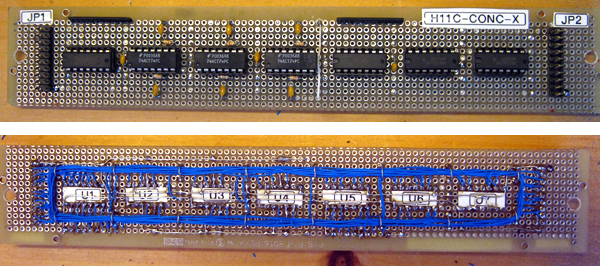
Debouncer board (H11C-CONC-X) was finished last night, being this the last hardware-related job until September. Hardware development is now on hold for the next two month.
Software and design related tasks, however, will continue; such as the production of the H1ASM assembler and the H1SIM simulator, and the re-design of the Master Controller board among others.
Reviewing the Instructions Set Architecture
06/20/2010
The current Instructions Set Architecture was designed nine months ago based on my early ideas about how instructions would be decoded using hardwired logic. I still think it's not a bad design, but it needs some adjustments and that's exactly what I am doing.
The new architecture relies, pretty much, on the same ideas, but it makes better use of bit-fields and it's better oriented to the decoding circuitry (yet to come). It is more rational, I think, and it also makes room for new instructions that I have in mind such as those for ALU operations with memory (not allowed by the current ISA) and increment/decrement instructions optimized for typical loops.
It is still pending how to produce long sequences such as the ones required for CALL and RET instructions (longer than 4 clock periods) but... I'm working on it.
The new (revised) Instructions Set is complete
06/26/2010
Finished to define and document the (revised) Instructions Set Encoding. It wasn't too hard but it was very tedious...
Also got to a solution for long sequences (instructions CALL, RET and INT) which take 8 cycles to execute instead of 1 to 4 cyles that all other instructions take.
Here is the resulting document:
http://www.armandoacosta.com/cpu/index.php?branch=576
Migrating to MS-DOS
06/27/2010
A few days ago I installed MS-DOS 6.22 on an old Pentium PC that I have and then copied to its hard drive my "glorious" probation of DOS stuff from my backup CDs. Needless to say that DOS is a lovely environment for old-fashioned tech people such as my self, so I got fascinated with the result.
What I love of working with DOS (rather than Windows or Linux) is the simplicity. You get things done quick and almost effortlessly; you have fewer choices so fewer things to worry about; you can focus on what you are doing with no distractions.
I was planing for C but the Microsoft Quick C ver 2 (QC2) that was once my war horse, were corrupted so for development I only have a copy of Borland Turbo Pascal 3.0... very limited but good enough for producing my assembler/simulator winning couple.
So it is decided: DOS will be the development environment for Heritage/1 software production. H1ASM will be rewritten in Turbo Pascal taking advantage of the good experience I had with the PHP implementation. The H1SIM simulator will also be written in Turbo Pascal... for DOS!
Working hard on the Simulator
7/8/2010
This simulator written in Turbo Pascal 3.0 proven easier than expected. In only six days (or nights...) of development it got to Fetch and Execute "real code" previously read into "memory" from a hex file.
I wanted it to look primitive, even more primitive than those programs that I used to write with Turbo Pascal twenty years ago. The text-only interface resembles the computer's console in a direct way, no fancy debugging commands have been added other than the ability to read a hex file from disk.
This primitive design has resulted in an intimate experience, very close to the machine being emulated which Console is expected to look more or less like this:
This program does not mimic the Heritage/1 exact circuits but only its behaviour. Hower, it resembles the hardware architecture at the block level, implementing in software the same solutions as in hardware. This match between software and hardware is giving me the oportunity to test those solutions on cold... which wasn't my initial intention, I have to confes...
Finished ISA review
7/15/2010
This simulator has proven to be a great "prove of concept" tool. It helped me to find inconsistencies in my Instructions Set that was more than happy to fix right a way.
Back to work
9/24/2010
I've taken this project back after a long pause and I've started by reviewing all of the "facts" most of them settled since many months ago. The architectural features are --I can see-- very mature at this point. Heritage/1 can definitely be described as a strict 16-bits "traditional" minicomputer based on single accumulator, single ALU, offering a --I would call it-- rich instructions set designed to execute simply and fast.
Features I really enjoy are the following:
- Instructions decoded by hardwired logic.
- Double-buffered registers.
- Not use of ROM
There are some features, however, that don't get to fit into the whole picture as for example the ability to disable the Timer by software (instruction DT: Disable Timer).
The idea behind the Timer was always the same it is still today: to assists a multiprogramming operating system in switching between processes. I've been always thought of the Timer as sort of "watch dog" sat there to make nearly impossible for a crashing process to hang the entire system... well, to try at least. So allowing routines to disable the Timer defeats its very purpose.
Today I decided to resolve the matter by getting back to the original idea that I've violated three month ago against my own sense of consistency. So, yes, I'm definitely removing instructions ET, DT from the Instructions Set as well as the TE flag (Timer Enabled) from the Flag's Register. Any solution for preventing critical-region code from being interrupted by the Timer's tic must be found within the OS design, not the CPU hardware.
It occurs to me, for example, that all system calls (issued asynchronically by processes) could wait in a "pending service queue" to be serviced later at "tic-time". Anyways, I'm not designing an Operating System yet so those issues will get actually solved in the future. For now I'm focusing in hardware design and I want it to be a clean one.
From Heritage/1 to LC-81
The dificult decision was finaly made
10/13/2010
Realizing that my spare time is getting more and more scarce, I put together a detailed list of all individual tasks pending for this project to sadly learn that it would take much longer that previously thought... about another year!
As other priorities came to my life I finally made the decision that I was trying to avoid: to put this project in "sleep mode" for an undetermined period of time.
I have to be honest: I feel like having divorced... However, a good thing about designing an old computer is that she never gets old, so I should be able to take it back some day, maybe when I retire.
LC-81 to the rescue
10/24/2010
Heritage/1 has been (and still is) a loved project; the only problem is the enormous amount of time and mental attention it demands from me. I was wondering what about to take something less demanding in terms of hardware design such as one based on an old microprocessor such as the Zilog Z80.
It is a totally different story, of course, but at least I could build a "basic hardware" in short, so I could devote the rest of the time to the second half of the matter which is Software and peripherals.
My problem with these kind of projects is that I take them very seriously in terms of "culture" and I've set my mind already around the "minicomputer culture".
Not entirely convinced yet, I nevertheless gave it a try. I called it "LC-81" to signify: a "Learning Computer", 8-bits, try 1.
Ready to wire
11/15/2010
LC-81 is a Mini-Computer based on Zilog Z80 microprocessor. I've missed the excitement of designing the CPU but gained, in return, a very fast development pace. In fact, the LC-81 "CPU Board" was designed in three weeks in contrast to Heritage/1 which took me one year to (partially) design the CPU circuits.
I also built the shassis for the "Lab implementation" of the machine. Here is a picture:
Now I'm ready to start wiring the boards starting with the "CPU Board" which contains the microprocessor, the first 16 KB of memory, bus buffers and some other logic.
A final words
11/30/2010
Heritage/1 is not dead, she's only sleeping as the Sleeping Beauty would... waiting for a prince with time!.
I believe that LC-81 will allow me to go faster in obtaining the experience necessary to tackle Heritage/1 in the future.... did I say correctly, future? Am I not building machines of the past?
I will stop posting notes on this site. Notes for the LC-81 project are in here:
http://www.armandoacosta.com/lc81/
|