ContentThis book contains early research notes as well as discarded ideas and solutions. Actually, content from anywhere in the site is moved to this book when it gets old.
The very first try
My first idea about building a homebrew computer were very ambitious. I expected to design a machine with hardware support for a multi-tasking protected UNIX-like operating system. This phase was greatly infuenced by Bill Buzbee Magic-1 project.
Overview
Heritage/1 is (or will be) a home-brew minicomputer made out of discrete MSI/SSI HCMOS chips and PLDs. It is designed to provide hardware support for Virtual Memory and Multi-Tasking. This book contains overall information about the project.
 The Computer The Computer
Main Features
Computer Name : Heritage/1
Data Bus : 16 bits
Address Bus : 20 bits (addresses point to 16 bit words)
Main Memory : SRAM 1 Mw (2 MB) max.
Arithmetic : Signed integer (two's complement)
Inst. decode method : Hard-wired logic using PLD chips
Operating Modes : Step, Real, Protected
Virtual Memory : Paging with Pages Tables in SRAM "Matrix" separate from Main Memory.
Page Frame size : 1Kw (2 KB)
Multitasking : Hardware support for up to 64 processes running in separate time-slices.
Software : None (Expected: Some Open Source Operating System)
Peripherals : Memory mapped
Interrupts : Vectored 256 max.
Nested ISR : Yes, based on priority
DMA : Yes
Technology : SSI/MSI HCMOS chips and PLDs
Construction : Prototyping boards with wires soldered (no wire-wrap) housing in 19" rackmount multi-card frames
Clock Speed : Pendig decision (expected: 12 MHz)
Computer Architecture
CPU Architecture
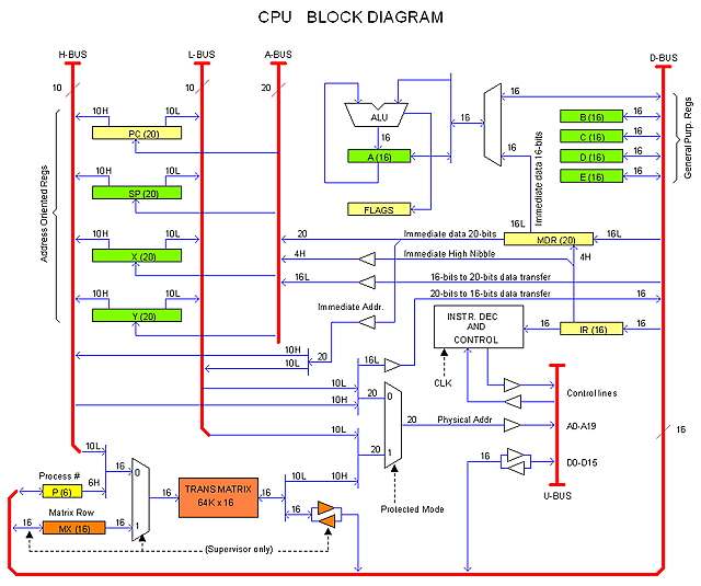
The figure below describes the Heritage/1 CPU architecture to the block level. I will explain how it works later. For now, you are invited to read my Notes. Remember that this design is in progress.
Registers
16-bits registers (Data oriented):
A Accumulator (Right operand and result for ALU operations)
B General purpose
C General purpose
D General purpose
E General purpose
20-bits Registers (Address oriented):
PC Program Counter (not directly addressable)
SP Stack Pointer (also a gernal purpose 20-bits register)
X Pointer for Indirect Address (also a gernal purpose 20-bits register)
Y Pointer for Indirect Address (also a gernal purpose 20-bits register)
Hidden Registers:
IR (16 bits) Instruction register
MDR (20 bits) Operand holder (both 16 and 20 bits)
FLAGS (?) Status flags
Supervisor Registers (Avilable in Real Mode. Also available for Supervisor code in Protected Mode):
P (6 bits) Current process when in Protected Mode.
MX (16 bits) Trans Matrix address
Important Note
This project is currenly on hold. I found that before continuing with a complex design such as that of Heritage/1, it would be better to start a simpler "pre-project" in which I could gain experience with basic Computer Design matters.
The info for the "pre-project" (currently in progress) is in the book titled PREHER-816.
The Project
Main Objective
The goal of this project is to design and build a minicomputer out of discrete components. The challenge is into provide sufficient hardware support for a true (Open Source) operating system than eventually could be ported in a further step.
Porting an operating system so it can run on a proprietary platform is a project per se for which I have no knowledge, no experience. So this is essentially self-educational project. Learning through research and experience in intimate proximity with all implementation details is actually the main objective of this computer project.
Current Status
06/11/2009
The project is officially on hold until I've gained sufficient experience while designing and building the "pre-computer" termed PREHER/816.
Project breakdown
I have broken the project into the following phases. I have not set dead lines because nobody if watting for it, but I can guess it will take quite a long time (one year at least).
Phase 1: Research
Start Date: 05/15/2009
I am thinking of a machine capable of running existing open source software on top of a ported UNIX-like kernel, but this may change. During this period I'll being acquiring the necessary background on computer design and operating system theory.
This phase will end up with specifications for the hardware design.
[End Date: 06/01/2009]
Phase 2: Hardware Design
Start Date: 06/02/2009
This phase will end up with a complete and detailed design of the machine's hardware.
Phase 3: Construction
This phase will end up with a functional machine with no software support. Code will be entered into memory by hand using the front panel switches. No signs other than LEDs will exists.
Phase 4: Experimenting with short routines
The machine built in Phase 3 will serve as a laboratory for testing different software approaches, entered by hand using the front panel switches.
Phase 5: Peripherals
At least one peripheral will be added to the machine for dumping code into memory. I am thinking of a RS232 port but this may change. Being able to dump large amount of code into the machine will allow me to experiment with more sophisticated code. This code, however, will still being assembled by hand.
Phase 6: Assembler
The manufacturing of development tools starts with this phase. I will be writing an Assembler. The purpose is to initiate my self into this specialized area and to gain experience for further development. Besides, I will need an assembler any ways.
This phase will end up with an Assembler capable of generate machine code for my computer.
Phase 7: Research on OS
In this phase I will be experimenting with development tools such as retargatable C compilers and trying to understand Opens Source Kernel's C code. I am supposed to have a good understanding of operating systems principles from Phase 1, so this is the time to put some hands-on.
At the same time, I will had gained sufficient experience with Linux and its development environment and tools. Must likelly I will be writting software using a Linux computer rather than a Windows one.
This phase will end up with a decision about what operating system to adopt. I am thinking of Minux or other UNIX-like OS but this may change.
Further
New phases will follow but this is not the time to anticipate it.
Specification for hardware design of the Heritage-1 minicomputer
06/01/2009
The present document specifies the hardware characteristics for the Herigage-1 home-made minicomputer.
Guidelines
1.- Modularity
The Heritage-1 minicomputer is housed into one or more units (enclosures) which in turn contain one or more PCB cards. The design must exploit such topology in order to allow for flexible configurations at both the unit and the overall system levels.
2.- Extensibility
Apart from the fact that the overall system can be extended by adding units and each unit can be in turn extended with new cards, each circuit inside a card (such as the ALU inside the CPU card) must be designed with extensibility in mind. For example, adding support for new arithmetic operations should not cause a total redesign of the CPU card.
3.- Concurrency
The Heritage-1 topology is naturally suitable for asynchronous concurring processing taking place over different units. This feature must be exploited in order to increase overall system efficiency.
4.- Reliability
Effort must be exercised to achieve reasonable reliability of the overall system. No new feature should be added at the cost of reliability descent.
5.- Reasonable performance
Although the Heritage-1 minicomputer is not meant to be fast compared with today's technology, annoying poor performance will not be acceptable. This must push to design to seek efficienty.
Part 1: General Description
The Heritage-1 is a home-made minicomputer designed to host a multi-user/multitasking Operating System yet to be either developed or ported from existing source code.
The machine can be operated in three possible modes: Step, Real and Protected. When not in Protected mode, all support for General Protection gets disabled thus low level code can be loaded and executed from anywhere in memory.
Main Features
Data Bus : 16 bits
Address Bus : 20 bits (addresses point to 16 bit words)
Main Memory : SRAM 1 Mw (2 MB) max.
Arithmetic : Signed integer (two's complement)
Operating Modes : Step, Real, Protected
Virtual Memory : Paging with Pages Tables separate from Main Memory.
Page Frame size : 1Kw (2 KB)
Multitasking : Hardware support for up to 64 processes
running in separate time-slices.
Peripherals : Memory mapped
Interrupts : Vectored 256 max.
Nested ISR : Yes, based on priority
DMA : Yes
Clock Speed : No specified
Technology : No specified
Memory Organization
Main Memory is wired for 16 bits data path. Addressing one byte separately is not possible in the Heritage-1.
When reading larger numbers (such as a 32 bits Long), the least significant word comes first, that is the smaller address corresponds to the least significant word composing the number.
Memory chips (either RAM or ROM) can be distributed in any manner within the addressable space, except for the following:
- The very first block of 512 words (00000-001ff) must be populated since interrupt vectors are pointing there. It is recommended to populate the entire 1 Kw page frame (00000-003ff).
- Not the entire (1Mw) addressable space can be filled with physical memory because peripherals are memory mapped. It is recommended to preserve 1Kw (the size of a page frame) for peripheral addresses, aligned respect to all other page frames.
Registers
Registers in the Heritage-1 CPU can be classified into three categories:
- General Purpose
- Address Oriented
- CPU specific
General Purpose registers are 16 bits and they are accessible to the applications programmer. The Accumulator (A) serves as left operand and result holder for the ALU.
Address Oriented registers are 20 bits and they serve as pointers to Main Memory or Peripherals.
CPU specific registers have different sizes and they are not directly addressable. Falling into this category are the Program Counter (CP) and the Instruction Register (IR).
Addressing Modes
This specification does not limit implementation of different addressing modes in the Heritage-1. However, it establishes the minimum to be provided. Those are the following:
Addressing Mode Example (pseudo assembler)
---------------------------------------------------------
Reg Immediate movi A, value
Reg Direct mov A, B
Mem Direct movd A, addr
Mem Indirect Indexed movx A, Y
Since peripherals are memory mapped, all memory addressing modes apply to peripherals as well.
Arithmetic and Logic Unit (ALU)
The ALU is designed so it can be enhanced with reasonable easy. The initial ALU must provide the following operations:
Note: All these operations apply to 16 bits signed (two's complement) integers.
ADD Add
DEC Decrement
CMP Logical NOT (complement)
AND Logical AND
OR Logical OR
XOR Logical XOR
SHIFT Both Left and Right with and without Carry
Instruction Set Architecture (ISA)
The Instruction Decoder and Control circuit (IDC) must be designed so it can be enchenced to support new instructions to come in the future.
The minumum instruction set must provide support for the following:
- Data transfers
- ALU operations
- Switching between Real and Protected operating modes
- Access to Supervisor operations when in Protected Mode
- Software Interrupts
The Heritage-1 computer allows code to access Supervisor privileged instructions when the machine is in Protected Mode as long as such code resides in page frames marked as Supervisor.
Interrupts
Interrupts are organized into 256 vectors termed INT-00 through INT-FF. The first sixteen (INT-00 through INT-0F) are for CPU internal use; all others (INT-10 to INT-FF) are available to peripherals.
Interrupt vectors points to consecutive locations in the very first block of the addressable space. Each vector takes two consecutive addresses, thus INT-00 points to 0x00000, INT-01 points to 0x00002 and so on. INT-FF points to 0x001fe.
When interrupted, the CPU fetches the corresponding vectored address. What is expected to be there is a branch instruction to the actual ISR.
INT-00 is the computer's clock tic raised at 1 ms intervals. A multitasking operating system can make use of INT-0 to define processes time-slices among other uses.
INT-01 through INT-FF are used by the CPU to generate exceptions. Software code is allowed to raise interrupts within this range by using interrupt instructions.
All interrupts are maskable. Not masked interrupts can be served in a nested fashion according to interrupt priority.
Queuing interrupt requests is the job of the Operating System. The CPU limits itself to service interrupts in the simple way we just described.
Peripherals
Peripherals are memory mapped and they may use interrupts for requesting CPU attention as well as DMA for direct data transfer to or from Main Memory.
Both Interrupt and DMA subsystems are designed in such a way that a peripheral cannot monopolize the bus during a data transfer operation. This is achieved by making the Computer's Clock Tic the highest interrupt priority of all so the Operating System can preemptively schedule all other interrupt service routine's tasks as well as DMA operations.
Part 2: Virtual Memory and General Protection
This section explains how The Heritage-1 computer provides hardware support for General Protection. The same is active when the computer is operating in Protected Mode; inactive otherwise.
Virtual Memory
When in Protected Mode, applications provide "Linear Addresses" instead of physical ones. A Linear Address is 20 bits wide and ranges from 0x00000 to 0xfffff with disregard of actual availability of physical memory. Linear addresses get eventually translated into physical ones as part of every bus cycle.
It follows that the system can commit to applications more memory than that physically available. Different techniques (such as Swapping) are employed to honor the commitment. However, such a job belongs to the Operating System whereas the CPU limits itself to provide the address translation mechanism and protection support, which is hardware-based.
Address Translation
Address translation is achieved by the mean of a circuit into the CPU called "Translation Matrix" (also called "Trans Matrix" or simply "Matrix") which is basically a 64K x 16 bits arrangement of static RAM. The Trans Matrix is separate from Main Memory and can be addressed by Supervisor code only.
From the Matrix viewpoint, physical Main memory is broken into 1024 blocks of 1024 contiguous addresses called "Page Frames". Each row in the Matrix represents a record (called "Matrix Entry") which holds information about a Page Frame.
The CPU circuitry sees Linear Address as divided into two fields:
A19-A10 : Page Number
A9-A0 : Offset
In combination (multiplex) with the current Process Number, the Page Number field addresses the Matrix to obtain a Matrix Entry which then provides the re-mapped (translated) 10 bits physical base address of the referred Page Frame. The Offset field of the Linear Address contributes in turn the 10 least significant bits to complete the final (physical) address put to the bus.
Note that Supervisor code can re-map Linear to Physical addresses at run-time by overwritting Matrix Entries.
Protection
Two means will ensure Protection via Matrix: (1) Control bits in the Matrix Entry, and (2) the "multidimenssionilty" of the Matrix.
Control bits are:
D15 S Supervisor The referred Page Frame is for Supervisor use only
D14 W Write The referred Page Frame can be written
D13 D Dirty The referred Page content have changed
D12 P Present There is a Page Frame associated to this record
D11 r (reserved) Not used
D10 r (reserved) Not used
Multidimensionality refers to the fact that the Matrix has N times P rows, where N=1024 is the total number of Page Frames in the Linear Space, and P=64 is the number of allowed symultaneous processes. Thus the Matrix provides each process with its own view (different dimenssion) of the same Linear Space.
The Operating System is expected to use these resources to provide General Protection.
Part 3: Construction
The Heritage-1 minicomputer is housed into one or more units (enclosures) which in turn contain one or more PCB cards.
Units
A unit is basically a multi-cards frame. It provides power supply for all cards but not to circuitry outside the unit. It also provides connectivity between cards and access to the External Bus (E-BUS). Some units also provide specific connections for specific needs.
The minimum configuration consists of the CPU Unit. It has at least two cards: CPU Card and Memory Card. There can be others such as a second Memory Card.
Other units to be added are:
- Storage Unit Hard drives, Flash Memory, etc.
- COMM Unit RS232 ports, Ethernet, etc.
Cards
All cards are pluggable and share physical dimensions, backplane connector type and pinout, etc. Details will be determined during the Design Phase.
A single card should devote to a single function in order to ensure modularity. For example, mixing CPU and Memory in the same card is not recommendable.
External Bus (E-BUS)
Units are connected through the External Bus (E-BUS). This multi-lines unified bus allows units to transfer information to each another in a Master/Slave fashion: At the time data is being transferred through the bus, only one unit is acting as the Master and only one unit is acting as the Slave.
The exact signals in the E-BUS, as well as cable type, connectors and pinouts, are to be determined during the Design Phase. The present document will only establish the minimum requirements for the E-BUS, which are the following:
- Provides Address and Data lines (either separate or multiplexed).
- Provides synchronization signals.
- Provides support for Interrupts.
- Provides support for Direct Memory Access (DMA).
- Does NOT provide power lines.
Requesting the E-BUS through Interrupts
The E-BUS provides two lines for managing interrupts: IRQT and IACK.
Devices request CPU attention by activating the IRQT line. The CPU grants the bus to the requester device by activating the IACK line. This last is connected in daisy-chain from device to device; devices that have not made the request pass the signal down to the chain; the device who made the request disconnects itself from the chain so the acknowledge signal can not propagate further.
Once the requester device is in control of the bus, it puts its interrupt vector on the Data lines and drops the IRQT signal. This vector had probably been set by DIP switches into the device at installation time.
When the CPU senses the IRQT dropped (with IACK still active), it reads the vector from the E-BUS, drops the IACK signal and calls the appropriate interrupt service routine (ISR).
Hardware Design step by step
This section contains notes written during the Hardware Design phase (June 2009) including partial tests done at the breadboard level.
Notes
Speed and components
The slowest component will set the speed of the computer, hence the need for picking the right kind.
CMOS 40xx series, for examples, are too slow, with propagation delays in the order of 100 ns. This is slower that most static RAM chips. HCMOS chips, in contrast, are very fast with propagation delays some times less than 10 ns (6 ns for 74HC00).
For registers, 74C374 gives me 165 ns from clock to latch. In contrast, 74HC374 gives me 20 ns. Same access time (20 ns) is found in SRAM 32Kx8 chip CY7C199CN from Cypress; I would use that chip for building the "Matrix" which is part of the CPU. 74LS series is even faster, but it is also more expensive; for my purposes, HC is OK.
As per PLDs, they are very fast. Amtel ATF22V10C for example (a good candidate for the Heritage/1) doesn't have any figure greater than 10 ns. Time from clock to output, for example, is 2 ns.
It seems then that the interval between control signals can be set around 20 ns. This makes a clock speed of 50 MHz, which is an impressive figure (I was thinking of 12 MHz before) but it's too early for making decisions about clock speed because no circuit have been designed yet. I just wanted to run some numbers and see where they would take me.
What is clear is that CMOS 40xx series are not use, so I shall employ HCMOS components instead.
Machine Cycles
Point, Open, Take
Any data transfer within the computer occurs always between two storage devices. By "storage" we mean any kind of device capable of holding data, such as a CPU register, a memory cell or an UART buffer.
Usually, the transfer takes three steps in time. First, both devices needs to be addressed. Second, the source devices needs to be opened to the bus. Third, the destination device needs to be clocked to latch the data from the bus. We call these steps: Point, Open and Take respectively. Each step has a duraction calculated to allow data to estabilize before commiting the operation.
The sequence of these steps is called a Machine Cycle (MC). There are different types of MCs as we shall see, but they are all essencially the same: Point (address), Open (three-state buffer) and Take (clock latch device). Some times we can skip one or two steps, making the MC shorter.
Fetch and Execute Cycles
In the following time diagram, T1, T2 and T3 constitute the steps mentioned before: Point, Open, Take respectively. Green traces represent sigals in bus lines whereas blue ones represent internal control signals (name indicated between brackets).
The naming convention for internal control signals is this:
OP_DEV
Where OP (operation) can be either RD (read, that is open the three-state buffer to the bus) or WR (write, that is clock the device to latch the input from the bus). And DEV (device) can be a register or any other storage device.
The diagram shows a complete instruction cycle for an indirect address operation. The memory location pointed by 20-bits register Y will be written from register A.
This instruction completes in two machine cycles: Fetch and Execute. The thing to notice is how different control signals appear in time to perform "Point", "Open", "Take" operations over different devices. The duration of T pulses should be big enough to allow data to stabilize before commitment.
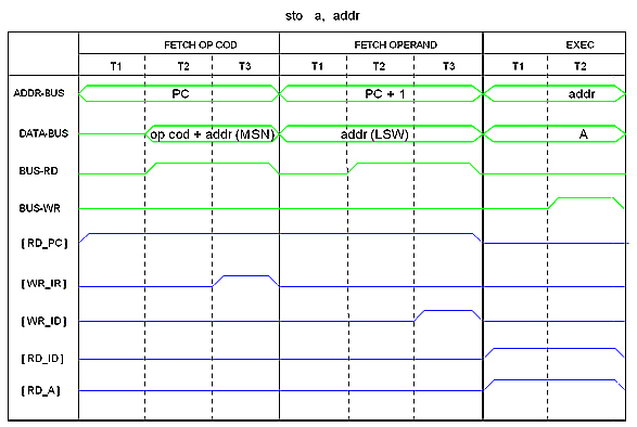
Fetch Operand Cycle
A memory-read cycle for 16-bits data reads a word from memory. An instruction such as
movi a, value ; a <- value (16-bits)
can complete in three machine cycles: Fetch OP-Code, Fetch Operand, Execute. For 20-bits operands, the mechanism is different. A 20-bits operand is needed for direct address instructions such as this:
sto a, addr ; [addr] <- a (addr is 20-bits)
It is also needed for Immmediate 20-bits instructions such as this:
movi sp, value ; sp <- value (20-bits)
In both cases, the least significant 16 bits word (LSW) of the 20-bits address or value is given in the word following the instruction. The most significant 4-bits nibble (MSN) is embedded within the OP-CODE. Thus such instructions can complete in three machine cycles as the following figure shows.
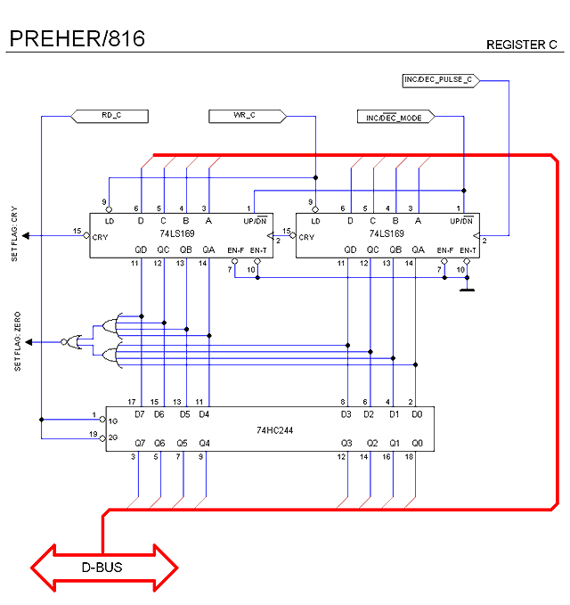
Control signals RD_ID and WR_ID applies to a special 20-bits register that I called "ID" in the drawing but I will call it "MDR" instead. Its sole mission is to hold the operand so it is available to the Exectute cycle. Yes, in the Heritage/1 the MDR register is the size of the Address Bus and there is no MAR register.
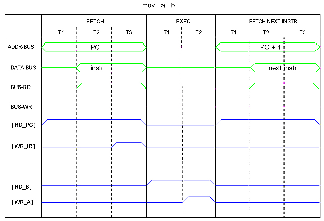
Register-to-Register
Transfer between registers don't require the "Point" step because registers are implicitly addressed by the OP CODE. In the time diagram below, EXEC machine cycle, T1 is an "Open" step and T2 is a "Take" step.
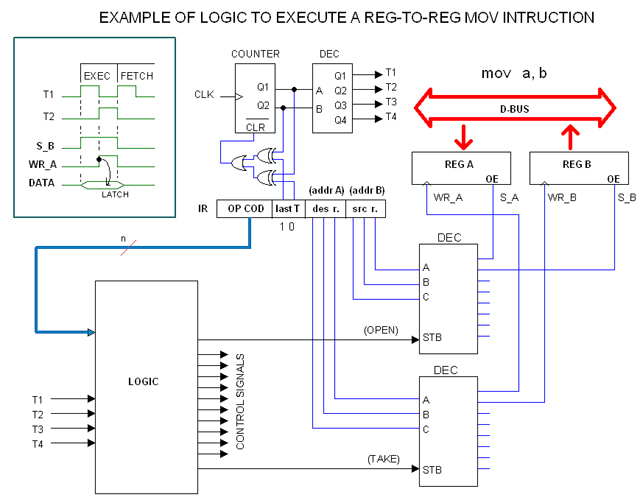
The following figure illustrates how this could be made in practice. Please know that this is not a definite design but only an illustration to the idea.
The instruction code shown in the figure presents two 3-bits fields to encode the destination and source register respectively. This bits are wired to respective decoders which in turn provide all S_reg. (select, that is, open) and WR_reg. (write, that is clock to latch) for all registers. In the example we have assumed eight registers in the CPU.
Note that one of these decoders (the one in the top) is dedicated to S_reg. signals whereas the other is dedicated to WR_reg. signals. The encoders also have an "strobe" input, so they will output nothing until the strobe signal is present and this comes from the Instruction Decoder Logic.
This logic takes the OP COD as input and it also takes the synchronization signals T1, T2, T3, T4. Those signals are obtaining from a 2-to-4 decoder fed from a 2-bits counter which in turn is clocked from the master clock.
We have seen that most instructions takes three steps (T1, T2, T3), but this takes only two. The solution is to provide a "shortcut" by reseting the counter so the decoder can jump to T1.
For that purpose, the Instruction have a 2-bits field termed "last T". The content is constantly compared with the counter output as we can see in the diagram. In this case, last T is equal 2, so as soon as T3 tries to appear, it will be forced to become T1.
The Logic is designed so signals S_B and WR_A appear as shown in the timing diagram. Then the counter is reset, as it is IR, so the next cycle will be, with no choice, a fetch cycle.
Register Increment / Decrement
Registers suitable for increment/decrement operations are implemented with binary counter chips. This means that increment/decrement instructions (such as INCR Y) do not involve data transfer and can be therefore performed in one single step, that is during T1.
Synchronizing with slow Peripherals
Peripherals for the Heritage/1 must be designed so they communicate with the Bus via three-state high-speed buffers such as the 74HC374. This is because the CPU will read and write the device (that is the buffer) at the same speed it does for static RAM memory. This means that, when reading from a peripheral, any delay introduced by the device itself must lie between the moment it is addressed and that in which the buffer got a valid data read from the device.
During this period (from addressing to data ready) the device must activate and keep active a bus line termed WAIT. The device will deactivate that line once the data has been safely transferred to the buffer.
The CPU samples the WAIT line during both "Open" and "Take" steps of every Memory Read cycle, that is T2 and T3 (remember that peripherals are memory mapped). If WAIT is active, the RD and WR signals are not activated, the IR register is not cleared and PC not incremented. This results into the same Machine Cycle being repeated over and over until the WAIT signal is removed by the device so the data (from the buffer) can be read as normal.
If an interrupt occurs while the CPU is waiting, it will be served. Upon return a new Machine Cycle will automatically resume the waiting condition.
Similar mechanism apply to write operations. The CPU will sample the WAIT line before rasing the WR signal in T2. Most likely the first time it will success since the data is written to a high speed buffer in the Peripheral circuitry. As soon as it is received, the peripheral will activate the WAIT line and will keep it active until it is ready for the next one. This implies that, when writting bulk data to a peripheral, the CPU will success the first but it will have to insert wait machine cycles for all others.
Proper design of peripherals will include, of course, the use of multibyte FIFO buffers. Those need to be 16 bits wide (the size of the Heritage/1 Data Bus); remember that this computer cannot address bytes individually.
The WAIT signal is then used to indicate buffer full condition.
Addressing Modes
The Heritage/1 features 16-bits general purpose registers and 20-bits address oriented registers. Such disparity makes transfers between registers of different sizes kind of odd. In order to fix this insanity I've came with RISC-like techniques leading to special immediate addressing modes for 20 bits registers.
Immediate 16 bits
This is the normal immediate addressing mode, common to most computers. It takes two consecutive words in memory: the op. cod. and the 16-bits operand.
Example:
movi a, value
Immediate 20 bits
To load a 20-bis register from memory would take two operands, but this would waste 12 bits from the second operand. The (RISC like) solution is to embed the most significant nibble (MSN) within the op. code. Therefore, an instruction of this kind takes only one operand from memory and can complete in two machine cycles.
Example:
movi sp, value ; Value is 20 bits but it only takes one 16-bits operand.
; the remaining 4 bits (MSN) is embedded in the op code.
Immediate 20 bits nibble high
When transferring data from a 16-bits register to a 20-bits register, only the 16 least significant bits are copied. The upper nibble can then be supplied by the mean of an "Immediate 20 bits nibble high" instruction which will write the 4 most significant bits leaving the rest untouched.
Example:
mov sp, a ; sp <- least significant 16 bits
movih sp, value ; sp <- most signifant 4 bits (value is 4 bits).
Immediate 20 bits nibble high intructions only takes one step (T1) of the Execute Machine Cycle since the operand is embedded within the op code. No bus operation is performed during this cycle.
The ALU/Accumulator partnership
In the Heritage/1 (as in most computers) the Accumulator register (A) holds the result of the last ALU operation. Additionally, it serve as a general purpose register. The ALU has two 16 bits inputs: A and whatever is in the Data Bus.
The figure below illustrates the relationship between A, the ALU and the Data Bus.
Control signal S_ALU (Select ALU) causes the ALU output to be routed to the Accumulator's input. When S_ALU is not active, the Accumulator is fed from the Data Bus instead so it can be used as general purpose register.
Signal S_A opens the Accumulator's output to the bus. We activate this signal when we want to read from A.
Signal WR_A clocks the Accumulator so whatever is at the input, gets latched. We activate this signal to write A from the Data Bus (example: mov a, b); the signal will actually commit the transfer. For performing logical or arithmetic operations, the same signal will commit the operation but in this case, S_ALU must be active.
Finally, the signal f (which takes n bits) defines the ALU operation to be performed.
We can see the ALU and the Accumulator as being part of the same circuit. The following figure illustrate such vision.
The signal S_ALU decides whether the box will behave as ALU or general purpose register A. In the lastest, signal S_A will be used to read from A whereas signal WR_A will be used to write (latch) toward A.
Register B is similar in the sense that the signal WR_B actually clocks its latches whereas S_B opens its three-state buffers to the BUS so others can read it. It is not shown in the figure but one can imagine.
Finally, here is a timing diagram of two operations with the A/ALU unit. We assume that f (not shown in the diagram) contains the code for the SUM operation.
During the first clock cycle, A is latched with the sum of itself and whatever is in the bus (B in this case). In a further clock cycle, B is moved to A.
The A/ALU unit will be most likely implemented with PLD whereas other registers will be built with 74HC374 chips.
Breadboard Testing
Test#1: Moving data between registers
For this test, I made 8-bits registers just for simplicity. In practice those will be 16 bits (using two 74C374 instead of one). Push buttons S_A, WR_A, S_B and WR_B simulate control signals (Select A, Write A, Select B, Write B respectively). Actually I did not use push buttons but momentary short-circuits made with wires. LED ON indicates logical 1; when "nothing" is in the bus, all LEDs go ON since bus lines are pulled-up to the power line (+5V).
The test went as following:
At the begin all LEDs were ON testifying a bus with all ones because of the pull-up resistors. By pressing S_A and S_B and could find what was stored at power-on into REG A and REG B respectively. They was all ones.
Using wires, I put some lines to ground in order to have some "data" over the bus. Then I pressed push button WR_A; this made my "data" to get latched into REG A. Then I remove the wires so the bus returned back to normal: all ones.
Now, I press S_A and S_B alternatively to see what is into REG A and REG B respectively. As expected, pressing S_A gave is my "data" back displayed by the LEDs; pressing S_B gave me the original all ones contained into REG B since the beginning of time.
The next step was to transfer my data from A to B. For doing that, I put the A content in the bus by pressing and holding S_A. In this conditions, I pressed WR_B momentarily. Finally I released S_A.
Now I repeated the regs reading by pressing S_A and S_B alternatively. Now both registers contained my data, as expected.
CONCLUSION
This test confirmed that I can build registers as planed: Wiring 74C374 chips as shown in the diagram (but combining two chips for 16-bits registers). It also confirmed the use of control signals S_X and WR_X for each register X.
Research Notes
These are the notes I made during the Research phase (May 2009).
Paging vs. Segmentation
05/21/2009
The title of this note is confusing; it suggests that Segmentation and Paging are mutually exclusive but that is not entirely correct. Those refer of alternate methods for managing virtual memory; however, modern processors such as Intel x86 provide support for both and is opt to the Operating System to use the one, the other or both.
Before entering into details, lets state that there are two ways (or "models") of seeing the virtual memory space: Linear and Segmented.
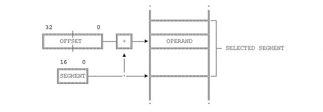
In the Linear Model, the virtual memory space is seen as an array of 2^32 (4G) bytes. To address it, a 32 bits pointer is all we need. The address provided this way is called a "Linear Address".
In the Segmented model the virtual memory space is divided into 2^16 segments, 2^32 bytes each. Two pointers are needed: One (16 bits) points to the segment; the other (32 bits) represents an off-set within the selected segment. This allows for a 2^(16+32) bytes (64 Terabytes). The address provided this way is called a "Logical Address".
|
We call this mechanism "Segmentation". A similar mechanism, "Paging", exists for organizing and managing memory in the Linear Model. Now lets get into details.
Since both models refer to virtual memory, some mechanism should exists to map virtual addresses into physical ones.
Segmentation (in the Segmented Model) maps the segment portion of the Logical Address to a physical memory address by the mean of tables called "descriptors". There can be a unique Global Descriptor Table (GDT), or one Local Descriptor Tables (LDT) per segment.
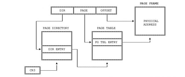
Paging (in the Linear Model) is performed by sub-dividing the 32 bits Linear Address into three fields called: Directory (10 bits), Table (10 bits) and Offset (12 bits), as shown below.
|
Two translation tables are employed for mapping the Linear address to a physical one: the "Page Directory" and the "Page Table". The Page Directory contains entries to the Page Table which in turn contains "a portion" of the physical addresses.
We said "a portion" because the physical memory is sub-divided into portions of 4K each called "Page Frames". The Page Table holds addresses for those page frames whereas the OFFSET portion (12 bits) of the Linear Address represents an off-set within the selected page frame.
Notice that as result of this paging schema we have up to 1024 directory entries each of which can contain 1024 pages, 4KBytes each, for a total of 4GB.
One may argue that the same job could be accomplished with just one table. The reason for the extra step is to handle the limited physical space with greater efficiency by making the size of the tables smaller.
When the two methods are used in combination, the Descriptor used by Segmentation does not hold physical memory addresses but Linear addresses which in turn get translated into physical addresses by Paging. In other words, each segment gets "paginated".
I have read that Linux prefers Paging to Segmentation because (1) it is simpler to implement and (2) because Linux is meant to be portable and some platforms such as RISC processors offer little support for segmentation.
The way for favoring Paging over Segmentation without losing the protection support offered by the processor trough Segmentation, is to use one segment only, then to implement Paging within that only segment.
More on Paging
The mission of Page Table entries is to describe Page Frames (not only to map them). Such description includes access rights, swap status etc. and it's used by the CPU to enforce general protection and to manage swapping, among other functions.
Each entry on a Page Directory (on a Page Table as well) consists of an array of 32 bits cconforming bit-mapped fields. We are not going to get into details but only to underwrite the following:
-- Each Page Table entry occupies 4 Bytes (32 bits). However, it describes a physical memory space of 4KB (one Page Frame).
-- Each Page Table occupies up to 4KB (1024 entries, 4 Bytes each).
-- Each Directory occupies up to 4KB too. In combination to the Page Tables it points, the Directory describes up to 1M page frames, that is, the entire 4GB linear address space as expected.
-- Page Directories and Page Tables hold the necessary information needed for the CPU to enforce protection.
An option for system designers is to allocate one global directory for each process running in the system. There are other options as well.
Learning from the PDP-11
05/31/2009
In this note I will mention those features of the PDP-11 that I am considering for adoption in my design.
Addressing words, no bytes
Unlike today's Intel microprocessors, in the PDP-11, addresses referred to 16-bits words, no 8-bits bytes.
Modularity
As most mainframe computers and minicomputers of the time, the PDP-11 consisted of separate units, but "Modularity" does not refers to this simple fact but instead to the way those units are interconnected in a flexible manner to allow for different possible configurations.
In the case of the PDP-11, modularity relayed on the UNIBUS.
UNIBUS
UNIBUS is a 56-lines path interconnecting all units together. It include Address lines (A0-A17), Data path (D0-D15), interrupt request lines (BR4-BR7), bus grant (BG4-BG7), Direct Access Memory (NPR), control and others.
Units use the UNIBUS to share information in a Master/Slave fashion. At any given time only one unit is in control of the bus (master) whereas other is serving as the slave. For example: the CPU as master and Disk drive as slave, or Disk drive as master and core memory as slave.
Bus access is negotiated between units by using Bus Request (BR) and Bus Grant (BG) lines according to a priority scheme.
Interrupts
Interrupts are organized into eight priority levels. The three lowest priorities are reserved to the CPU but this can be set (by software) to a highest one.
UNIBUS lines BR4-BR7 are used by devices for requesting bus control (interrupt). Devices connected to BR7 have the highest priority and so on.
Bus grant lines (BG4-BG7) are connected in daisy-chain. When the CPU grants bus control as result of a BR request, the associated BG signal is propagated from device to device along the chain. That device who issued the interrupt cuts the chain so the grant signal can not be propagated further.
Then, the device takes to bus and puts a memory address to it; that address is where the interrupt service routine resides. What the CPU does in response is just to load the Program Counter (PC) with that address to initiate a fetch bus cycle.
The CPU only serve interrupts which priority is greater that the one it has. For example, if the CPU has been set to priority 7, no interrupt will be served.
Interrupts can be nested, observing the priority scheme described above.
First Approach to Implementation
Simplified Memory Management
05/23/2009
The justification to simplify existing Memory Management techniques is that I want to explore those concepts in a manageable way so not get lost with complicated details. After all, it is not my intention to produce a commercial computer.
Physical Memory
Physical memory is wired in 32 bits rows meaning that the data bus is 32 bits wide.
However, physical addresses refer to 8 bits chunks. For example, the address range: 0x01 - 0x10, represents a zone of 16 bytes, not 64 bytes. This is done by making the address bus from A31 to A2 as in the Pentium processors. Unlike Pentium, however, I will not allow bus cycles to get 8 nor 16 bits; instead, all bus cycles will always read or write a 32 bits row (four bytes at once).
This arrangement dictates (or suggest) other decisions such as: Instruction code must be 32 bits, CPU registers must be 32 bits though "splitable" into 16 and 8 bits so different data types can be available to the programmer, etc.
Linear Model
Applications will see memory as a Linear space of 2^32 bytes (4GB). As for physical memory, each increment in the Linear address represents one byte, not one 32 bits row. For example, for getting 8 contiguous bytes, the application may issue the following linear addresses: 0x01, 0x05 (not 0x01, 0x02).
Application code will be linked to produce linear addresses. Often, same addresses will appear repeated among different applications running simultaneously at a given time. For the CPU, however, application addresses represent nothing but offsets (indexes) within the designated space which only translate to physical addresses at the very bus-cycle time (by hardware).
Each application will believe that it owns the entire 4GB linear space. This illusion will connect to reality at translation time into the CPU circuitry.
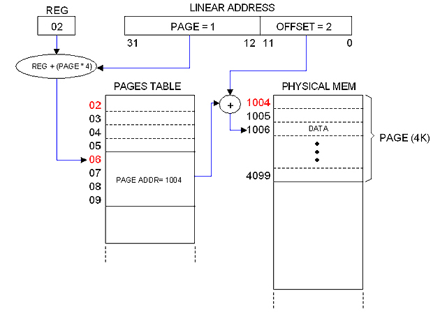
Paging
The image below illustrates my simplified paging mechanism which mission is to implement linear-to-physical Address Translation and Global Protection.
The linear address is broken into two fields: PAGE (20 bits) and OFFSET (12 bits). This allows for 2^20 pages, 4KB each.
Pages are described in the PAGE TABLE. Each entry in the table takes 4 bytes representing bit-mapped fields. One of these fields (20 bits long) is the "Page Address" which is the base physical address for the referred page. The other fields are used for Protection.
The PAGES TABLE entry is obtained from the PAGE field of the Linear Address and a certain register (REG) which hold the base address for the Table. The PAGE field actually represents an index.
The OFFSET field of the Linear Address provides the index within the given physical page to compute the translated physical address, as illustrated in the diagram.
One Pages Table for each running process
Since, as mentioned, each process believes to own the entire linear address space, one Pages Table for each process is needed. I will cover this in a separate note dedicated to Processes.
The 4MB frontier
The Pages Table can be as small as 4 bytes or as big as 4MB. However, its natural size is 4KB (one page frame) because that is the granularity of memory allocation.
A Pages Table of 4KB has 1024 entries which describes 1024 pages, that is, 4MB of physical memory. Hence 4MB becomes a "natural frontier" for physical memory.
Therefore, it sounds natural to establish that the machine's memory will be expandable in steps of 4MB. Besides, 4MB of static RAM is about $100 at today's prices... definitely a reasonable frontier!
Limitation of my one-step paging mechanism
The Pages Table occupies a contiguous space in physical memory. It can expand to a maximum of 4 MB (2^20 entries times 4 bytes) but in practice it will be shorter since entries will be added as memory gets allocated.
This design imposes a limitation to the size of the Linear space: It cannot be greater that the greater physical address available. Otherwise, I will be forced to popultate the entire 4MB table to accomodate all possible linear addresses.
The system can still commit more memory than the physical memory available. What it cannot is to commit a Linear address for which an entry in the Pages Table does not exist.
That is the price to pay for my simplified one-step paging mechanism.
First approach to Paging implementation
05/23/2009
In previous note (Simplified Memory Management) I suggested that Pages Tables will take room from physical memory address space, but that is not true.
-- NOTE: --
I've borrowed most of the terminology from Intel literature but that "Pages Table" sounds ugly to me... I will call it "Translation Table" from now on, or simply "Trans Table".
-----------
I mentioned that it should be one separate Trans Table for each running process (since each process should be into believe that it owns the entire linear space). If I content my self to limit the number of simultaneous processes to a practical value, then I can afford to build a separate "room" in the CPU, out of the addressable RAM, to host all Trans Tables ever needed.
Let set the limits:
-- Max number of simultaneous processes: 128
-- Max RAM size: (Conceptually: 4 GB) expandable in steps of 4BM.
The "room" will be a SRAM matrix of 128K x 32 (using four 128K x 8 chips) expandable in steps of 128K x 32 (four chips). I will call this: the "Trans Matrix" or simply "Matrix".
Each row in the Matrix represents a Trans Table entry. With 4MB of RAM in the computer (1024 pages), 1K rows covers the entire linear space for that amount of physical memory. Therefore, with 128K rows at my disposal I can give one entire Trans Table to each of the 128 allowed processes.
As mentioned, expansion is possible (and easy). The only thing is that, as RAM expands, the Trans Matrix must be expanded accordingly. It would be better, maybe, to place the Matrix on the memory card, disributed among them in case that more than one exist.
System software is responsible for populating the Matrix. I will create the appropriate Supervisor instructions for doing that. Please notice that the Matrix needs to be updated as processes get alive and die, not only at boot up time.
Close up to the Trans Matrix
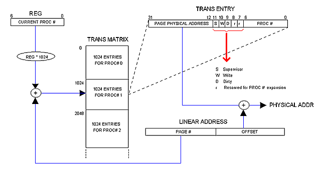
05/23/2009
The following diagram illustrates how the Trans Matrix participates in address translation and protection.
The Matrix holds a record (1024 rows deep) for each running process. Each record constitutes the process Trans Table, that is, the space available for the process to allocate the 1024 possible Trans entries.
Each process has a process number (PROC #). The current proc # is kept in certain register (REG in the diagram) as long as the process is running. That number is used as an index to access the corresponding record. The PAGE field of the Linear address is used, in turn, as an index within the record to locate the exact Trans Table entry.
As mentioned in previous notes, the Trans Entry contains the physical base address for the page in physical memory. It also contains the following control fields:
S Set if the page is for Supervisor use only
W Set if writing on this page is permitted
D Set is the page have been modified
r Reserved for future expansion
PROC # Process number
There is a reason for including the PROC #.
I mentioned in a previous note (Limitation of my one-step paging mechanism) that the Linear space available to applications is limited far below 2^32. If a buggy code submits a linear address that exceeds the limit, chances are for the Address Translation mechanism to compute an entry that is valid but belongs to the wrong process. To avoid this, the CPU will always verify that the PROC # field matches the content of REG before proceeding with Address Translation. Besides, stamping each process page with the Proc# seems to me an elegant way of assuring that inter-processes interferience will not occur.
Scalability Issue
05/25/2009
I've being thinking all the time of a static and moderate (16MB at the most) main memory distributed among different cards, 4MB each.
Lets say, however, that one day I decide to build a card with 8MB instead of 4BM. In such a case, I'll dimension the Trans Table chuck accordingly (just for that card), hence the advantage of a distributed Trans Matrix.
Problem starts when memory increases far beyond "moderation". Imagine that one day I decide to play with dynamic memory and to build a card with 256 MB of dynamic RAM. The Trans Matrix chuck for that amount of memory becomes 8M x 32, that is: 32 MB of static RAM! (about $900 at today's prices).
There are several ways for working this issue out:
1.- Reducing the limit for running processes (currently 128).
2.- Not event thinking about large amount of memory.
3.- Discarding the solution all together.
First approach to Memory Allocation
05/24/2009
Linear and Physical domains
When we express memory addresses as Linear (0 to 2^32 -1) we say them to be in the "Linear Domain". Addresses expressed as physical (as wired in the circuit) are said to be in the "Physical Domain".
Since Linear-to-Physical address translation is done as part of the bus cycle (using the Trans Matrix), the physical domain is mostly restricted to that low level context. General purpose registers and even the PC (Program Counter) manage Linear Addresses instead of Physical ones. We can say that "our CPU works in the Linear Domain".
Memory allocation, however, is done in the Physical Domain since it involves Trans Matrix population and efficient ways of using the available physical memory, as we shall see.
Memory Allocation
The unit of memory allocation is the Page Frame (4KB of contiguous bytes in physical memory). For the CPU, an alloc operation involves not much but adding entries to the Trans Matrix. Once in the Matrix, referred pages can be accessed throughout the Paging mechanism at the CPU circuit level as part of the ordinary bus cycles.
The CPU must provide a supervisor instruction similar to this:
mem_alloc page, control
Where:
Page Physical address of the Page Frame
Control Bitmapped control fields and PROC #.
System software is responsible for keeping track of allocation. This involves (among others):
-- Distribution of physical memory among different processes (Effort must be made to avoid collisions).
-- Finding the correct physical blocks size for efficient use of memory.
-- De-allocation
Contiguousness in Linear and Physical domains
We have to distinguish between contiguous Linear address and contiguous Physical addresses. A code segment without branches, for instance, always occupies a contiguous block in the Linear domain but not necessarily in the Physical domain as illustrated in the following image.
This will possibly be a common scenario in real life. Notice that memory fragmentation is hidden to the program code (which is in Linear domain), meaning that System software working with these issues must work in the Physical domain instead. Hence the need for Physical-Domain instructions provided by the CPU.
Allocating Processes
When a process is loaded, memory is allocated to store the code and leave room for the process data. Since I am not providing support for a segmented model, both code and data will share a monolithic block in Linear space.
The upper portion (lowest addresses) contains the code; the data block follows and extends all the way down to the bottom of the designated space.
At loading time the Data block is only the space remaining in the last page occupied by the code. The process code is responsible for requesting memory to the OS is needed. The OS will allocate requested memory as contiguous as possible just below. This way, the space designated to the process will grow indefinitely only limited by the amount of physical memory available at allocation time.
The way processes utilize their data space is opt to the language Compiler. The OS and/or the CPU can help with support for different techniques (stack, heap, etc) but they won't dictate the way programming languages manage their data.
Linear Relative Address (RLA) and Program Counter (PC)
We have established that applications believe they own the entire Linear space. Such a believe is more than an illusion: actually, there is no other Linear space but that given to the application at run-time. We can see the Linear space as being "multi-dimensional": The Trans Matrix contains all its "dimensions": one for each application running at a given time.
It follows that applications supply only Linear addresses and those are not absolute but relative to the beginning of the designated block in memory. In other words, the CPU interprets addresses supplied by the application as offsets within the designated code-data block. We call this a "Relative Linear Address" (RLA).
Application code is linked to produce RLAs. The first RLA (where execution starts) is always cero. The address where the Data block starts (following the Code block) is known at Link-Time, so addresses for instructions such as "MOV A, ADDR" can be resolved by the Linker and they are also given as RLAs (relative to the beginning of the Code block).
This has implications to the Program Counter (PC).
Fetch bus cycles will perform address translation from a given a Linear address. But we just said that application code always starts in address cero. Since (at application run-time) there is no Linear space other than the one owned by the application, then the RLA becomes the actual address to be fetched. Therefore, the content of PC can't be other but the RLA provided by the application code.
When paging is enabled (that is, when not in Kernel mode) there is no need for a CS register. No need for a DS register either. I can still provide support for stacks (a SP reg and associated PUSH/POP instructions, for example) but that will be a plus, not strictly required by the conceptual model.
Second approach to implementation
05/26/2009
In this second try, I'm bassically scalling down the first to manageable values.
Critics to my first approach
My "First approach to implementation" failed to meet expectations. Here is why.
32 bits architecture
There is no need for a 32 bits architecture. The aim of 32 bits address space with 32 bits data path was only in to leave enough room for further development. However, the figures ran close to unfeasibility so I've decided to restrict the architecture down to reality. After all, it is not my plan to compete with my PC but just to create a hardware environment to play with.
The all-for-one commitment policy with 32 bits
I have adhered to this principle from the very beginning. It stated that every application running in protected mode must believe it owns the entire Linear address space, that is all memory in the system (and yet that not physically present) up to 4GB (2^32).
I still consider it's a good idea. Problem is that 32 bits are too many bits. That, combined with the multi-dimensional Trans Matrix, ran out of reality big time.
Code and Data in monolithic block
Putting code and data together in same block under the application's control makes it difficult to share process's images among different users.
In a multi-user environment same process should be able to run on behalf of different users at the same time, so the process's code must be shared among them but the data must not. It follows that it's better to keep code and data in separate areas perfectly distinguishable by the Operating System for easier manipulation.
Brief description of the "new machine"
Here is how the machine starts to looks like:
Data Bus : 16 bits
Address Buss : 24 bits
Main Memory : SRAM up to 16 MB
Virtual Linear Space : From 0 to 2^24 - 1
Paging mechanism : 128Kx16 SRAM Translation Matrix not in Addr Space.
Max symultaneous processes : 32
All-for-One Policy
As stated before, the System commits all Linear address space to each application running at a given time. User applications are linked to produce Linear Addresses relative to the beginning of the designated code block, starting with address cero. Maximun address is 2^24 - 1.
Linear Address and Paging
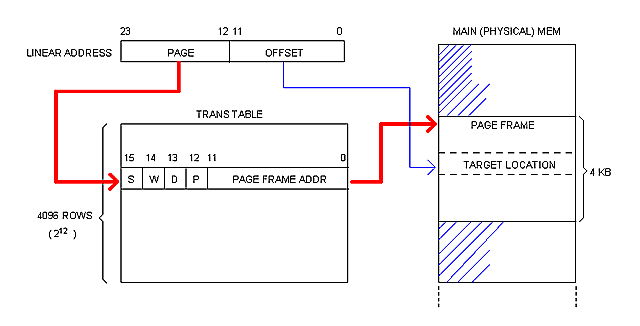
A Linear address is 24 bits wide. It is broken into two 12 bits fields: PAGE and OFFSET.
Physical memory is broken into 4 KB blocks of contiguous addresses called "Page Frames". The page frame constitutes the memory allocation unit.
Each page frame is described (and translated) by the corresponding entry (or "Frame") in the Trans Table, as illustrated bellow.
Each process processes its own Trans Table. System Software (OS) is responsible for keeping them updated at boot-up and run-time.
Multi-dimensional Trans Matrix
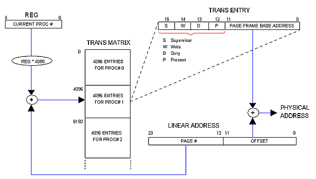
Trans Tables are not in Main memory but in a separate circuit called "Trans Matrix" (or simply "Matrix") which is 16 bits wide and 128K rows deep regardless the amount of physical memory installed in the machine.
The Matrix is said to be "multi-dimensional" because it contains the Trans Tables for all 32 allowed processes. This way, each process runs in its own "dimension" of the Linear space. The OS distributes physical memory among processes dynamically by filling in the Matrix.
The following diagram illustrates how it works.
( + ) and (REG * 4096) circles are shown for illustrative purposes only. In practice REG will simply contribute the most significant bits to the Matrix row decoder whereas the PAGE field of the Linear address will contribute the least significant ones. Same for: PAGE FRAME BASE ADDRESS + OFFSET = PHYSICAL ADDRESS.
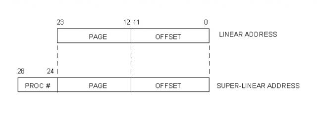
Super-Linear space
Unlike user processes, that always work in Linear space (within its own "dimension"), Kernel code needs access to all processes memory meaning that it needs access to the whole Trans Matrix.
With this purpose, we define a "Super-Linear Space" that ranges from cero to the size of the Trans Matrix times the size of a page frame.
Using the limits we have established, the size of the Super-Linear Space can be calculated like this:
SL_Size = (Page_Frame) (Trans_Table_Entries_per_Process) (Max_Processes)
= (4KB) (4096) (32)
= (2^12) (2^12) (2^5)
= 2^29
= 512 M
The following diagram illustrates the relationship between Linear and Super-Linear address.
Paging in Kernel mode
05/27/2009
Since Trans Tables are not in Main memory, there is no need for defeating Paging when Kernel code is running. Moreover, keeping Paging active brings advantages to the Kernel's job.
Let's assume that the Trans Matrix has been pre-initiated by some pre-Kernel software possibly hold in ROM chips. This initiation regards only the first Trans Table: that of the Kernel. Yes, Kernel code resides in virtual space so it suffers address translation as everyone else. Kernel is nothing but "Process #0".
There is something special about this Kernel area, however: The CPU is designed so all interrupts are serviced from Trans Table #0, that is Process #0 which is the Kernel.
This has implications to System Calls.
When a process needs Kernel attention, it raises INT 80 (the number 80 is just an example, matching Linux in this case). Call arguments are passed in CPU registers, as expected.
In some cases, arguments represent pointers to memory (a buffer, a stru file descriptor, etc). The question is what kind of "memory address" does this pointer represent: a Physical address or a Linear Address?
We have established that processes only deal with Linear addresses so that is the only kind of address it can pass in a System Call. The Kernel code would then have to make a translation (to physical address) based on information it holds about the calling process.
With Paging enabled, the translation is almost automatic.
Say for instance that the calling process has passed a buffer's address where it wants data to be placed. This will be a Linear address pointing (relative) to somewhere within the process's data block. Let's call it LOCAL_BUFF.
In order to know where to serve the requested data, the Kernel needs to compute a "Super Linear Address" which translation matches the physical address of LOCAL_BUFF. Let's call it BUFF and calculate it like this:
BUFF = (PROC# * 4096) + LOCAL_BUFF
Now, by simply addressing the Matrix with BUFF, the exact Physical address is automatically obtained. In other words, the user's buffer has been addressed via ordinary bus cycle with Paging enabled.
We see that "Kernel mode" is not a strong concept any more; Kernel pages are marked as Supervisor which allows access to special CPU instructions, that's all. We see also that Paging does not need to be enabled or disabled; all buss cycles can be done in the same way by using the Matrix.
One may argue that the Kernel will need to fill in the Matrix any ways with physical addresses so it must be able to work in the Physical domain. One answer may be that the Matrix is only accessible through special supervisor instructions since it is not in addressable space; thus Kernel code could manage to know the Physical memory without having to actually address it; as a matter of fact the Matrix maps the Physical Memory in some way.
I can't have this as a final conclusion, however. For one part, that is not the way real-life Kernels and processors work; for the other, I haven't explored all of the consequences with full detail. Moreover, being this an "experimental" computer, it is better for me to have as many choices as possible, as for instance the ability to enable/disable the Paging mechanism.
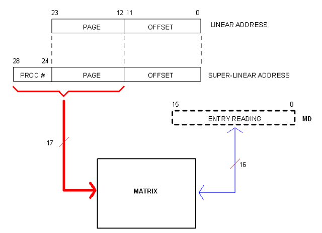
Addressing the Matrix
05/28/2009
I were thinking of a set of privileged instructions as the only way to access the Matrix. But now it occurred to me that a more open (so powerful) mean would be to allow Kernel code to simply address the Matrix.
Of course, Kernel code will be doing so in Super-Linear space. However, only the most significant 17 bits of the (29 bits) Super-Linear address are needed since the other 12 represent the off-set within the page frame (as in Matrix entries). The following diagram illustrates the idea.
Register MD is not a real one but a fictitious resource provided by the CPU to facilitate Matrix Read/Write operations as in (for example):
MOVI MD, value
CPU the first Sketch
05/29/2009
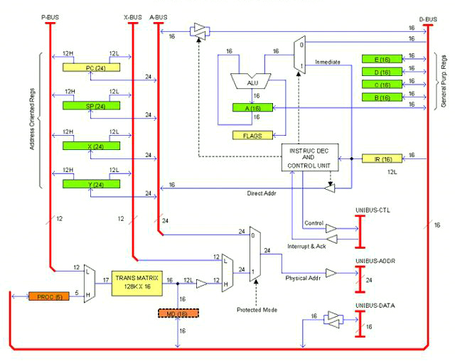
The following drawing is an early sketch (actually the first) of the CPU architecture or block diagram, whatever you want to call it.
This is supposed to be a single PCB card. As per today I don't know if the computer will take one or more units (enclosures); several cards, for sure. The idea is that all cards (and/or units) will be plugged to a common bus that I have called UNIBUS (as that of the legendary PDP-11, not sure if I'm going to adopt exactly that bus).
The UNIBUS consist of Data lines (16), Address lines (24) and Control lines including IRQs. In the drawing they are termed: UNIBUS-DATA, UNIBUS-ADDR and UNIBUS-CTL respectively. This is the way out for the unit (or Card).
There are also internal buses. Those are: D-BUS (16 bits Data), A-BUS (24 bits Address), X-BUS (12 bits Offset) and P-BUS (12 bits Page). These buses communicate registers and other resources inside the CPU card.
Registers can be classified into three categories:
- General Purpose: A, B, C, D, E
- Address Oriented: PC, SP, X, Y
- CPU specific: IR, FLAGS, PROC, MD
There is also the Trans Matrix.
General Purpose registers are 16 bits and they are accessible to the applications programmer. The Accumulator (A) serves as left operand and result holder for the ALU (as in must real-life processors).
Address Oriented registers are 24 bits. They have bidirectional access to the A-BUS and split one-way access to the P-BUS and the X-BUS. In the drawing, each line is marked with the number of bits it carries; when split, an H or L suffix added to the number indicates whether it is the Most or Least significant half.
CPU specific registers have different sizes. IR (16 bits) is the Instruction register; FLAGS is the Status register. When the CPU is in Protected mode, the register PROC (5 bits) indicates the current process number. MD is a fictitious register that represents the current Matrix entry.
The Matrix is a SRAM arrangement of 128K rows by 16 bits. It is addressed by the combination (multiplex) of PROC and the P-BUS. The 12 least significant bits of the selected row represents the physical base address of the Page Frame to be addressed in the current bus cycle. By multiplexing this output with X-BUS (which contributes the Offset) the whole 24 physical address is obtained. If the CPU is in Protected mode, that address is taken to UNIBUS-ADDR; otherwise, the A-BUS content is taken instead.
In the drawing, registers are marked with different colors to highlight privileged use. Green registers are accessible to the Applications programmer. Orange registers are only accessible to System programmers (that is, if the CPU is in Protected mode, code cannot access these registers if it is not in page frames flagged as "Supervisor"). Yellow registers are indirectly accessible throughout instructions; for example, a jump instructions overwrites the Program Counter. When the CPU is in Real mode, page priviledges are not checked so orange registers are accessible to all code.
Note that register PROC is for System programmers use. That is the way for Kernel code to work in Super-Linear space (I'm keeping my idea of the Kernel working in Protected mode but this may change).
Some implementation details are not clearly illustrated in the drawing as for example the rules for transferring data between registers of different sizes. There is a number of different ways of doing that but I'm not going to work it out at this time.
Calculating the Matrix
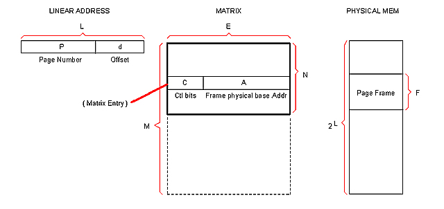
The size (thus the cost) of the Matrix has proven to be a critical concern. Lets imagine a generic Matrix so we can adjust values until acceptable results are obtained.
These are the variables:
L : Size of the Linear addressable space.
P : Size of the PAGE field in the Linear address.
d : Size of the OFFSET field in the Linear address.
F : Number of addresses composing a Page Frame in physical memory
E : Size of a Matrix entry.
A : Size of the FRAME_ADDRESS field in the Matrix entry.
N : Number of Matrix entries per Table (that is, per process).
S : Number of max simultaneous processes.
M : Total number of Matrix entries (for S processes).
Note: Sizes are in bits.
Here are the relationships between those variables:
d = log2 (F) ; Number of bits needed to address F
P = L - d ; A linear address has L bits
A = P ; This conclusion is easy to obtain
N = 2^P ; The Trans Table has as many entries as P can address
M = N * S : The Matrix has as many tables as allowed sim. processes.
Procedure
We start by fixing the size of the Linear space (L) since that will determine the max amount of physical memory allowed in the system.
Then we fix the size of the page frames (F). Here is a trade-off situation: The smaller is F, the bigger becomes the Matrix; but making F too big will degrade memory management efficiency. We can start with a reasonable value (say, 4KB).
With these two variable fixed, we can start doing the math
#Linear Address fields:
d = log2 (F) ; Number of bits in the OFF_SET field
P = L - d ; Number of bits in the PAGE field
#Matrix entry:
A = P ; Number of bits in the FRAME_ADDRESS field.
The Matrix entry also has control bits (about 4) and can also contain reserved bits. What we do is to add them all, then we round to a multiple of 4 (for practical reasons). Extra bits resulting of rounding will be considered "reserved".
#Trans Table size:
Trans Table is the chunk of Matrix dedicated to one process. The number of entries is:
N = 2^P
So far we have a Matrix that is N rows by A bits... per process.
#Matrix size:
The Matrix has as many trans tables as simultaneous processes are allowed (S). This is another trade-off situation. In this step we fix S seeking a comfortable value with acceptable cost in Matrix RAM.
M = N * S
The final size of the Matrix is M rows by A bits.
Example
Let Main Memory be 2MB as the most. Therefore L = 21.
With such a small memory lets keep granularity high, say 1 KB per frame, that is: F = 1024.
#Linear Address fields:
d = log2 (F) = 10
P = L - d = 21 - 10 = 11
#Matrix entry:
A = P = 11
We have 4 control bits so the entry would be: 11 + 4 = 15 bits. Since this is kind of odd, we round to 16 bits and tell programmers we have let a "reserved bit", which sounds very technical.
#Trans Table size:
N = 2^P = 2048
So we have 2K x 16 bits (4KB) per process.
#Matrix size:
Let say we want to allow up to 128 simultaneous processes.
M = N * S = 2048 * 128 = 262,144
That is 256 Kwords (512 KB).
If we can afford to build this Matrix, then our system can be described as following:
- Main memory : 2 MB max
- Sim. Processes : 128 max
- Matrix size : 256K x 16 bits (512 KB).
(not too bad...)
Third Approach to Implementation
05/31/2009
This approach derives from my Second Approach to Implementation, now narrowed to more definite values. In addition, a promising interrupt scheme has been introduced.
Features
Data Bus : 16 bits
Address Bus : 20 bits (address refers to 16 bit words)
Main Memory : SRAM 1 Mw (2 MB) max.
Operating Modes : Step, Real, Protected
Protection Method : Paging via (not mapped) Multidimensional Matrix (16K x 16)
Multitasking : Up to 16 processes running on separate time-slices.
Peripherals : Memory mapped
Interrupts : Vectored 256 max.
Nested ISR : Yes, based on priority.
Interrupts
Interrupts are organized into 256 vectors termed INT_00 through INT_FF. The first sixteen ones (INT_00 through INT_0F) are for CPU internal use; all others (INT_10 to INT_FF) are available to peripherals. Vectors point to memory addresses in the very first block of the addressable space taking two consecutive addresses per vector as we shall see.
Nested interrupt service is allowed according to vector priority. INT_00 has the highest priority whereas INT_FF has the lowest.
Hardware
The external bus (E-BUS) provides two lines for managing interrupts: IRQT and IACK.
Devices request CPU attention by activating the IRQT line. The CPU grants the bus to the requester device by activating the IACK line. This line is connected in daisy-chain from device to device. Devices that have not made the request pass the signal down to the chain; the device who made the request disconnects itself from the chain so the acknowledge signal can not propagate further.
Once the requester device is in control of the E-BUS, it puts its interrupt vector on the Data lines and drops the IRQT signal. This vector have probably been set by DIP switches into the device at installation time.
When the CPU senses the IRQT dropped (with IACK still active), it reads the vector from the E-BUS, drops the IACK signal and calls the appropriate interrupt service routine (ISR).
Software
Interrupt vectors points to consecutive locations in the very first block of the addressable space. Each vector takes two consecutive addresses; thus INT_00 points to 0x00000, INT_01 points to 0x00002 and so on. INT_FF points to 0x001fe.
For servicing an interrupt, the CPU will do nothing but a fetch bus cycle toward the corresponding address. What is expected to be there is a branch instruction to the actual ISR.
INT_00 is the computer's clock tick, raised at 1 ms intervals. A multitasking operating system can make use of INT_0 to define processes (or threads) time-slices.
INT_01 through INT_FF are used by the CPU to generate exceptions. Software code is allowed to raise interrupts within this range by using the INT instruction.
All interrupts are maskable. Not masked interrupts can be served in a nested fashion according to interrupt priority.
Queuing interrupt requests is the job of the Operating System. The CPU limits itself to service interrupts in the simple way we just described.
External Bus (E-BUS)
All units connect to the External Bus (E-BUS) which is made of two multi-pair cables (termed A and B) ended with D-SUB 25 pins connectors at both edges. A and B cables interconnect units in daisy chain topology.
These are the signals present in each cable. The actual pinout has not been defined yet.
CONNECTOR A
=====================================================
A00-A19 Address lines
GND Signal Ground
CONNECTOR B
=====================================================
D0-D15 Data path
IRQT Interrupt Request
IACK Interrupt Acknowledge
DMAR Direct Access Memory Request
DMAK Direct Access Memory Acknowledge
BBSY Bus busy
DTWR Data Write
DTKE Data Take
GND Signal Ground
Power lines are not provided in the bus so units are required to be self-powered.
Signals DMAR and DMAK are similar to IRQT and IACK but they work with Data Access Memory (DMA) rather than interrupt.
Signal DWRT determines whether the bus cycle if for reading or writing (from the Master viewpoint). It is active for write cycles.
Signal DTKE will usually be connected to Output Enable pins (OE) of three-state chips. Actual data transfer occurs when this line is activated.
The 8-bits "pre-project" (PREHER/816)
Before the Heritage/1 will be the PREHER/816, which is (or will be) a very basic 8 bits minicomputer with no support for virtual memory, multitasking nor protected mode. Its mission is to teach me the very basis of computer design: how to build registers, muxes and bus controllers, for example.
The Computer
Main Features
Computer Name : PREHER/816
Data Bus : 8 bits
Address Bus : 24 bits external (16 bits internal)
Main Memory : Up to 16 MB SRAM distributed in 256 banks 64 KB each.
Arithmetic : Signed integer (two's complement)
Inst. decode method : Hard-wired logic
Real-Time Timer : Computer "tic". Interrupts the CPU at 1ms intervals
Peripherals : Memory Mapped
Interrupts : (Decision pending)
DMA : (Decision pending)
Technology : SSI/MSI HCMOS chips (Considering: PLD)
Construction : Prototyping boards housed in home-made multi-card frames.
Clock Speed : (Decision pending; expected: 12 MHz)
Architecture
The PREHER/816 minicomputer consists of several cabinets called "units" joined together by a common bus called U-BUS. Units are home-made multi-cards frames. The U-BUS, though composed by data, address and control lines, looks like a single multi-wire cable ending in DSUB connectors.
Units can be combined in flexible ways to make different configurations. The most basic configuration consists of one CPU unit. Practical configurations will include the STORAGE unit (Hard drives) and the COMM unit (RS3232 and Ethernet). More units can be developed as needed.
CPU
The CPU Unit (a home-made multi-cards frame) has two buses in the backplane: the A-BUS (16 address lines) and the D-BUS (8 data lines). Different cards connect to those buses. Other connections such as internal control signals also exists between cards. The U-BUS is the external bus; only the "Bus Controller Card" is connected to it. The U-BUS is not present in the backplane.
The CPU architecture is pretty classical. The register A (accumulator) serves as left operand and result for the ALU. It is not possible to obtain ALU results in a register other than A. What it is possible, however, is to transfer data between 8-bits and 16-bits registers using instructions such as: "movh b, y".
The register MB (Memory Bank) provides support for a memory banking scheme allowing for 16 MB of memory divided in 256 banks of 64KB each. Note that the internal address bus (A-BUS) is 16 bits so the banking scheme is optional and has no impact to the rest of the architecture.
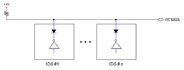
There is not MDR/MAR registers but a 16-bits MDAR register which sole mission is to hold the operand for immediate and direct addressing modes instructions. The Instruction Decoder and Sequencer (IDS) is hard-wired (no micro coded) implemented with PLD chips.

|
Registers
8-bits registers (Data oriented):
A Accumulator (Right operand and result for ALU operations)
B General purpose
C General purpose
D General purpose
E General purpose
16-bits Registers (Address oriented):
PC Program Counter
SP Stack Pointer (also a gernal purpose 16-bits register)
X Pointer for Indirect Address (also a gernal purpose 16-bits register)
Y Pointer for Indirect Address (also a gernal purpose 16-bits register)
Hidden Registers:
IR (8 bits) Instruction register
MDAR (16 bits) Operand holder (both 8 and 16 bits)
FLAGS (?) Status flags
Addressing Modes
-Register : Data is conteined in given register
�Examples : mov a, b ; A <- B
: movh a, sp ; A <- SP (MSB)
-Immediate : Data if given in the byte(s) following the op. cod.
�Examples : movi a, data ; A <- 8-bits data
: movi sp, data ; SP <- 16-bits data
-Direct : Data is in the memory location which address is given in the two bytes following the op. cod.
�Example : ld a, addr ; A <- [addr]
-Indirect : Data is in the memory location which address is contained in register X or Y
�Example : ldx a, x ; A <- [X]
-Stack : Data comes from the Stack (always pointed by register SP)
�Example : pop a ; A <- [SP]; SP <- SP-1
-INC/DEC : Register is incremented or decremented in a sigle clock cyle (no data transfer occurs).
�Example : dec c ; C <- C-1
Tech Info
Instruction Decoder and Sequencer (IDS)
The following block diagram illustrates the idea of our hardwired Instruction Decoder and Sequencer (IDS) but first, lets establish the following:
1.- The op. cod. is 8-bits wide and does not contain bit-mapped fields; it is basically an "instruction number".
2.- Instruction cero is not a real instruction but the number for the Op Cod Fetch cycle. Therefore we have room for a maximum of 255 instructions.
3.- Op Cod Fetch cycle takes 3 periods (T1, T2 and T3).
4.- Execution takes 1 to 9 clock periods, depending on the instruction. If more than one machine cycle are involved (for instance, an instruction with operands) we count its periods consecutively without breaking between machine cycles. For example, the instruction "LD A, addr". (load register A from memory location at address "addr") will be fetched during T1, T2, T3 and then executed during T1, T2, T3 (addr LSB operand), T4, T5, T6 (addr MSB operand), T7, T8, T9 (actual execution).
5.- Most instructions will exectute in two or three clock cycles. Only instructions with two-bytes operands will takes the longest exectuion time (9 clock cycles).
Now, the diagram.
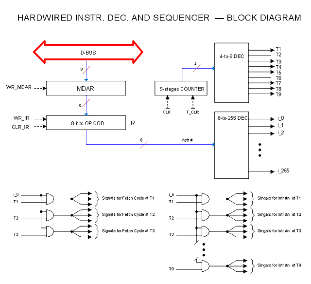
|
The whole purpose of this circuit is to obtain the exact control signals that we need for each clock cycle (T) for each instruction (i). In this view, Op Code Fetch (i_0) is just a particular case.
Note that the instruction byte is not read directly from the bus into the IR register but in the MDAR register instead. This is because we need the OP COD to be available along the entire life of the instruction cycle; we would lose it otherwise when reading an operand from the bus. When reading operands, they are read into MDAR while IR keeps the op cod for the rest of the instruction cycle. Signals WR_MDAR (latch into MDAR from the bus) and WR_IR (latch into IR from MDAR) are not simultaneous but separated in time by half a clock period.
We obtain signals T1 ... T9 (instruction "age") from the main clock, as illustrated. Separately we obtain signals i_0, i_1 ... i_255 (instruction being processed) from the op code.
For each instruction implemented in the CPU there is a simple logic similar to the one shown. It just combines each i_n signal with each Tm signal to provide the control signals needed for instruction, for time. In particular, there is a logic for i_0 (lower left corner in the diagram) which produces the sequence for the Op Code Fetch Cycle.
Signals internal to the IDS such as WR_MDAR, WR_IR, CLR_IR etc. are generated too from these little logic blocks. In particular each instruction must end its sequence by clearing the counter (T_CLR) which forces the appearance of T1, and clearing the IR register (CLR_IR) which forces the next Fetch Cycle.
Schematics
Register C
06/13/2009
This is a first attempt to implement registers that can be incremented or decremented without ALU operation so INC/DEC intructions execute in one clock cycle (Signal INC/DEC_PULSE_C).
The 16-bits Heritage/1
I finally decided to forget about that "OS ready" minicomputer and make PREHER/816 (renamed back Heritage/1) the main subject of my project. I also decided to make my machine 16-bits so it is suitable for some useful work in the future.
Tech Info
This book will describe the computer in great detail. For now, it contains the most recent versions of circuits and ideas.
Conditional Status and Flags Register
The Conditional Status describes the result of a data operation. This can be (not exclusive):
Zero (Z): if the result is zero
Negative (N): if the result is negative
Carry (C): Arithmetic carry
Overflow (V): if the result does not fit into the destination
The S-BUS
Since the Conditional Status refers to a result and this is always kept in some register, detecting status is a job for the register's circuitry. Therefore, each register offers its own means for detecting its own Conditional Status.
The way for registers to deliver their individual status to the Flags register, is by the mean of a 4-bits bus (wired in the Data Slots) called S-BUS.
All registers are constantly generating status signals internally but, at a given time, only one is open to the S-BUS. This is because Flags should only be set according to the register being accessed by the current instruction and only if that instruction is meant to affect flags.
An exception to this rule are those instructions that increment or decrement two registers at the same time (INCM, DECM and INDEC). In this case both registers open to the S-BUS and flags are set as an "OR" of the individual conditions.
There are none dedicated control signals for opening registers to the S-BUS. The selection is made automatically when the register in question is Loaded, Incremented or Decremented.
Registers that do not report status
Registers that are not meant to hold results, won't report conditional status (they are not wired to do so). Those are the following:
-- Program Counter (PC)
-- Stack Pointer (SP)
-- Operand Register (OR)
-- Instruction Register (IR)
The Flags Register (F)
The Flags register (F) resides in the Master Controller card (MC) which plugs to both Data and Control slots. The register is 8-bits but only 4 are used to remember the Conditional Status; a 5th. bit is used to remember the Interrupt Enabled condition as we shall see; the remaining 3 bits are implemented but not used (reserved for future use). The whole register F is saved to the Stack during CALL or Interrupt and restored back upon Return.
The register is actually made out of D-type flip-flops (74ACT74) fed from the S-BUS. The outputs go to another bus (called CS-BUS) wired in the Control Slots; this bus is always open so the current status is always available to Controller cards. Flags are latched selectively using signals LD_FZ, LD_FN, LD_FC and/or LD_FV produced by IDS cards during the last cycle of those instructions that affect flags.
Instructions and Flags
Although further analysis on this topic is still pending , I can anticipate the following:
-- ALU instructions affect all flags (Z,N,C,V).
-- Data transfer instructions (MOV, LD, STO, PUSH, POP) affect flags Z, N.
-- Increment/Decrement instructions affect flags Z, N, V.
-- Branch instructions affect none flag.
By not affecting flags, I mean that the previous status remains. The programmer needs to take this into account when placing conditional branch instructions within the code.
The Interrupt Enabled condition
The necessity of recording the Interrupt Enabled condition as a flag has to do with nested interrupts. When an interrupt service routine (lets call it: ISR1) gets interrupted by a highest priority interrupt (ISR2), the Interrupt Controller disables interrupts before passing control to ISR2. If this routine failed to enable interrupts back, then interrupts would remain disabled when control returns to ISR1, which is not the intended behavior. But, by remembering the Interrupt Enable condition in the Flags register, interrupts will be automatically restored upon return since F had been saved to the Stack.
Thus there is a flip-flop in F for the Interrupt Enable condition, only that its input (SI) and output (CSI) are not wired with the S-BUS and CS-BUS respectively but treated as point-to-point connections. This is because only a few circuits will make use of them; those circuits are: the Interrupt Controller, the IDS card responsible for the DI and EI instructions and the Control Panel.
CPU BACKPLANE
The CPU backplane is constructed on a prototyping board holding six 96-pins DIN41612 female connectors and other six 120-pins DIN41612 female connectors. This divides the backplane into two sections: Data Slots and Control Slots respectively. The former is used for "data oriented cards" (such as registers) and the latest is used for "controller cards".
Each of the two Slot types are wired separate. Most of the wires conforms different buses whereas others serve for point-to-point inter-card connections.
A special card named "Master Controller" features two connectors (one 96-pins and the other 120-pis) and plugs to both Slot types. This card contains those circuits that need access to the two worlds such as the Instruction Register (IR), the "Arbitrer" and others. It also provides the interface (buffering) with the external bus (U-BUS).
Following is the pinout for both Slot types:
Data Slots
- - - - - - - - - - - - - -
A B C
- - - - - - - - - - - - - -
1 GND GND GND
2 D0 PP D8
3 D1 PP D9
4 D2 PP D10
5 D3 PP D11
6 D4 PP D12
7 D5 PP D13
8 D6 PP D14
9 D7 PP D15
10 L0 PP L8
11 L1 PP L9
12 L2 PP L10
13 L3 PP L11
14 L4 PP L12
15 L5 PP L13
16 L6 PP L14
17 L7 PP L15
18 RST PP L16
19 FLT PP L17
20 SZ PP L18
21 SN PP L19
22 SC PP L20
23 SV PP CLK
24 A7 PP A15
25 A6 PP A14
26 A5 PP A13
27 A4 PP A12
28 A3 PP A11
29 A2 PP A10
30 A1 PP A9
31 A0 PP A8
32 +5V +5V +5V
- - - - - - - - - - - - - -
Signals Descriptions:
DO-15 Internal Data Bus
A0-15 Internal Address Bus
L0-20 Internal Lamps Bus
SZ Set Conditional Status Zero
SN Set Conditional Status Negative
SC Set Conditional Status Carry
SV Set Conditional Status Overflow
RST System Reset
CLK System Clock
FLT Fault Condition
PP Point-to-Point Control Signals
Control Slots
Except those marked as "PP" (Point to Poin), all signals in Control Slots are wired together in a Bus.
Signals marked as CTL (Control) are not designated yet but they will as the design progresses.
- - - - - - - - - - - - - -
A B C
- - - - - - - - - - - - - -
1 GND GND GND
2 IR0 PP IR8
3 IR1 PP IR9
4 IR2 PP IR10
5 IR3 PP IR11
6 IR4 PP IR12
7 IR5 PP IR13
8 IR6 PP IR14
9 IR7 PP IR15
10 CTL CTL CTL
11 CTL CTL CTL
12 CTL CTL CTL
13 CTL CTL CTL
14 CTL CTL CTL
15 CTL CTL CTL
16 CTL CTL CTL
17 CTL CTL CTL
18 RST CTL CTL
19 FLT CTL CTL
20 CSZ LD_FZ CTL
21 CSN LD_FN CTL
22 CSC LD_FC CTL
23 CSV LD_FV CLK
24 CTL CTL CTL
25 CTL CTL CTL
26 CTL CTL CTL
27 CTL CTL CTL
28 CTL CTL CTL
29 CTL CTL CTL
30 CTL CTL CTL
31 CTL CTL CTL
32 CTL CTL CTL
33 CTL CTL CTL
34 CTL CTL CTL
35 CTL CTL S1
36 CTL CTL S0
37 CTL CTL EOE
38 CTL CTL ET1
39 CTL CTL ET0
40 +5V +5V +5V
- - - - - - - - - - - - - -
Signals Descriptions:
IR0-15 Instruction Register Output
CSZ Conditional Status Zero
CSN Conditional Status Negative
CSC Conditional Status Carry
CSV Conditional Status Overflow
LD_FZ Load Flag Zero
LD_FN Load Flag Negative
LD_FC Load Flag Carry
LD_FV Load Flag Overflow
S0, S1 Operational Status
ET0, ET1 Enconded Time (T1, T2, T3, T4)
RST System Reset
CLK System Clock
FLT Fault Condition
CTL Control Signals (Bus)
PP Control signals (Point-to-Point)
Encoded Time:
- - - - - - - - -
ET1 ET0 Time
- - - - - - - - -
0 0 T1
0 1 T2
1 0 T3
1 1 T4
- - - - - - - - -
Operational Status:
- - - - - - - - - - - - - - - - - - - -
S1 S0 Operational Status
- - - - - - - - - - - - - - - - - - - -
0 0 Halt
0 1 Fetch
1 0 Execute
1 1 Interrupt being negotiated
- - - - - - - - - - - - - - - - - - - -
Operation
The Heritage/1 is operated similar to 1960's and 1970's minicomputers. When powered-on, the computer has no software in it so it does basically nothing.
Once the computer is powered-on, the operator uses the Console to load the desired software from storage. Before doing that, however, a little "loader" program needs to be entered manually using the Console's Entry switches.
The Console
The Heritage/1 Console is very simple. It consists of two parts: The bottom half is designed for "programming", that is entering code into main memory. The upper half is designed to facilitate low level software and circuitry debugging.
The computer can operates in four different Operational Modes: RUN, SLOW, STEP and PROGRAMMING. It can also be Halt. The desired Operational Mode can be set from the OPERATIONAL MODE block. After power-on or reset, the computer is in Halt condition.
While in RUN mode, the computer operates at full speed. In SLOW mode, the system clock is replaced with a very slow one (several Hertz) which frequency can be adjusted using the rotary knob. When in STEP mode, the computers halts after the current instruction has finished execution; pressing the STEP button again causes the next instruction to be fetched and executed. When putted in PGM mode, the programmer block at the bottom can be used.
Bus content and different control signals are constantly monitored by LEDs no matter the current Operational Mode. The DATA and ADDRESS LEDs monitor the internal Address and Data buses respectively. Specially useful is the FAULT LED which lights to indicate a CPU exception condition. After a fault, the computer halts automatically.
Working in Programming Mode (PGM)
To enter Programming Mode, the operator presses the PGM button in the OPERATIONAL MODE block. Buttons in the PGM block illuminate to indicate that they can now be used (they are ignored in RUN and SLOW modes). The ADDRESS and DATA LEDs now show the address and content respectively from the default memory location; this has been set using an internal DIP switch.
Buttons EXAM- and EXAM+ can be used to navigate the memory from that point back and forward respectively. For each time, a memory read cycle is performed for updating the LEDs reading. If a different address is needed, this can be entered using the ENTRY switches, then pressing the ADDR button. The ADDRESS and DATA LEDs will then show the new address and content respectively.
To modify memory content, the operator enters the desired value using the ENTRY switches, then he presses the DTA button; this causes the new content to be written to memory and the address to be automatically incremented. This implies that, upon DTA button pressed, the address and data shown in the LEDs correspond, not to that just modified but to the one immediately next.
If, for instance, the operator wants to fill a block of memory with a given fixed data value, he needs to proceed as following:
1.- Enter the desired base address in the ENTRY switches.
2.- Press the ADDR button. Both address and memory content will be displayed.
3.- Enter the desired data in the ENTRY switches.
4.- Press the DTA button. Address and content for the next memory location will be displayed.
5.- Press the DTA button repeatedly as many times as needed. For each time, the current location will be written from the switches and the address will be incremented automatically.
A more practical example is to enter a "loader" program that allows the computer to load an existing application from storage.
Once the memory has been modified as desired, the operator enters the initial program address in the ENTRY swithes, presses the ADDR button and then presses the RUN button to star running the program. It can also chose to run the program in SLOW or STEP modes.
The computer can be halt at any time by pressing the HALT button in the OPERATIONAL MODE block.
Low-level Debugging (HALT)
When the computer is in Halt condition, switches in the REGISTERS CONTROL and BUS CONTROL blocks can be used. They are ignored otherwise.
The REGISTERS CONTROL block allows the engineer to load, increment, decrement, open to the internal data bus (D-BUS) or to the internal address bus (A-BUS) any of the CPU registers. The BUS CONTROL block allows to manually manage the external U-BUS control signals. Eventually the computer can be ran completely manual from those blocks. Even a system clock can be asserted by pressing the Halt button.
We can also write content to internal A-BUS and D-BUS from the ENTRY switchers. Now, the EXAM- and EXAM+ in the PGM block are not operational so they are not illuminated. ADDR and DTA buttons, however, are illuminated to indicate that we can used them, only that in different manner respect to that in Programming Mode.
Whatever is in the ENTRY switches can be passed to the internal D-BUS by pressing the DTA button in the PGM block. The switches content will simply be opened to the D-BUS, not written to memory. The value will not be latched either, so we will need to press and hold the DTA button as long as we need it to be present in the bus. The previous also applies to the A-BUS and the ADDR button.
Running a program (RUN, SLOW, STEP)
Running a program is different depending on the previous Operational Mode.
If the RUN (or SLOW or STEP) button is pressed while the computer is in PROGRAMMING mode, then the initial address is the one entered in the ENTRY switches. To run a program this way the operator needs to enter the initial address with the switches, press the ADDR button, then to press the RUN (or SLOW or STEP) button to initiate execution.
If the RUN (or SLOW or STEP) button is pressed while the computer is in HALT condition, then the initial address is that contained in the Program Counter register (PC). To run a program this way, the engineer loads the initial address into PC, then presses the RUN (or SLOW or STEP) button to initiate execution.
BUS LAB
Before going further, I will build this development tool that I called BUS LAB. It is basically a manual-signals generator and monitoring tool that will provide control signals (Switches) and will monitor buses status (LEDs) to be used in circuits under testing.
Operation
Though designed with the Heritage/1 in mind, this BUS-LAB is a generic tool (I think).
Once connected to the LAB, buses in the target circuit are constantly monitored by LEDs in the BUS MON block of the LAB's front panel. Additional (8) signals can be monitored in the AUX block.
ENTRY SWITCHES write data to the selected bus. Switches labeled "OE" in each bus open a 3-State buffer from the switches to that bus. Caution must be observed for not to open more than one of the OE switches as the same time.
The switches and LEDs in the REG CONTROL block provide manual control signals to the different registers. Switches in the AUX block can be used for same purpose.
Finally is the CLOCK section at the bottom. The "CLK SRC" switch selects the source for the clock; this can be either an oscillator provided by the LAB or the CLK switch. The resulting clock signal is monitored by the CLK LED.
Power (regulated 5V) is provided too. This is monitored by the "+5V" LED.
Buses and the CPU Backplane
Heritage/1 units are interconnected via an external bus called U-BUS; each unit in turn possesses its own specific internal bus. Within a unit, all inter-card connections are made via a Backplane made of 96-pins DIN 41612 connectors. Two different kinds of connections exists: buses and point-to-point; this implies that frame slots are not generic but dedicated, that is cards cannot be placed anywhere within the frame but in their designated slots.
CPU internal busses are: D-BUS (data), A-BUS (address), S-BUS (conditional status flags), C-BUS (internal control signals) and T-BUS (instruction sequence count). A Bus Controller Card not plugged to the Backplane but placed behind it, provides the necessary interface to the external U-BUS.
External Bus (U-BUS)
The U-BUS consists of two ribbon cables termed A and B respectively, ended with D-SUB connectors that plug from unit to unit in Daisy-Chain topology. Signals in the U-BUS are the following (NOTE: The actual pin-out has not been defined yet):
CABLE A (D-SUB 25)
- - - - - - - - - -
ADDR LOWER : A0-15
ADDR UPPER : A16-23
CABLE B (D-SUB 37)
- - - - - - - - - -
DATA : D0-15
CONTROL : MRD, MWR, MWT, IRQ, IAK, BSY, SRT
RESERVED : Future use (13)
Power (+5V) is not present in the U-BUS since units are self-powered.
Control Signals in the U-BUS
MDR: Memory Read
MWR: Memory Write
MWT: Wait (for synchronization with slow devices)
IRQ: Interrupt Request
IAK: Interrupt Acknowledge
BSY: Bus busy (not in 3rd. state)
SRT: System Reset
Note: Peripherals are memory mapped.
CPU Internal Bus (Backplane)
CPU Backplane slots are classified into two classes: DATA SLOTS (for data oriented cards such as the ALU and registers cards) and CONTROL SLOTS (for controller cards such as IDS and Interrupt Controller).
The pin-out adopted is identical to the industrial standard VME Bus P1, except for those signals not used in the Heritage/1. Point-to-point signals and Heritage/1 specific buses have been added in place of those.
Data Slots
The table below shows the resulting pin out for DATA SLOTS. Signals labeled CTL are for point-to-point connections mostly internal control signals. Some other signals have been added such as: SR (System Reset) and CSZ, CSN, CSC (Conditional Status Zero, Negative and Carry, respectively).
A B C
- - - - - - - - - - - -
1 DO CTL D8
2 D1 SR D9
3 D2 CTL D10
4 D3 CTL D11
5 D4 CSZ D12
6 D5 CSN D13
7 D6 CSC D14
8 D7 CS3 D15
9 GND CS4 GND
10 CLK CS5 CTL
11 GND CS6 CTL
12 CTL CS7 CTL
13 CTL CTL CTL
14 CTL CTL CTL
15 GND CTL CTL
16 CTL CTL CTL
17 GND CTL CTL
18 CTL CTL CTL
19 GND CTL CTL
20 CTL GND CTL
21 CTL CTL CTL
22 CTL CTL CTL
23 CTL GND A15
24 A7 CTL A14
25 A6 CTL A13
26 A5 CTL A12
27 A4 CTL A11
28 A3 CTL A10
29 A2 CTL A9
30 A1 A0 A8
31 CTL CTL CTL
32 +5V +5V +5V
Control Slots
For Control Slots, same control pins plus the 16 address lines (not used by IDS cards) are wired in three local control buses: C-BUS, S-BUS and T-BUS. Lines D0-15 are not wired from the internal Data Bus as in Data Slots but directly from the Instruction Register (IR).
The table below shows the pin out for Control Slots.
A B C
- - - - - - - - - - - -
1 DO SF D8
2 D1 SR D9
3 D2 S0 D10
4 D3 S1 D11
5 D4 CSZ D12
6 D5 CSN D13
7 D6 CSC D14
8 D7 CS3 D15
9 GND CS4 GND
10 CLK CS5 IE
11 GND CS6 CTL
12 ET0 CS7 CTL
13 ET1 CCS CTL
14 ET2 CTL CTL
15 GND CTL CTL
16 CTL CTL CTL
17 GND CTL CTL
18 CTL CTL CTL
19 GND CTL CTL
20 CTL GND CTL
21 CTL CTL CTL
22 CTL CTL CTL
23 CTL GND CTL
24 CTL CTL CTL
25 CTL CTL CTL
26 CTL CTL CTL
27 CTL CTL CTL
28 CTL CTL CTL
29 CTL CTL CTL
30 CTL CTL CTL
31 CTL CTL CTL
32 +5V +5V +5V
Control Bus (C-BUS)
The purpose of wiring all control signals in a bus is to allow different controllers (such as IDSs and the Interrupt Controller) to manage the same control lines as illustrated in the figure below:
Status Bus (S-BUS)
SF Fetch Cycle
SR System Reset
S0 Operational Status
S1 Operational Status
CSZ Conditional Status Zero
CSN Conditional Status Negative
CSC Conditional Status Carry
CS3 Conditional Status (Reserved)
CS4 Conditional Status (Reserved)
CS5 Conditional Status (Reserved)
CS6 Conditional Status (Reserved)
CS7 Conditional Status (Reserved)
CCS Clear Conditonal Status
IE Interrupt Enabled
SF signal is activated by instruction decoding logic (located at IDS cards) during the falling edge
of the last clock cycle of every instruction. The signal is used to syncrhonically clear both IR and the T-Counter; this action forces an Op Code Fetch Cycle taking place with the next clock rising edge.
S0, S1 define the current Operational Status according to the following table:
- - - - - - - - - - - - - - - - - - - - - - - - - - - - - - -
S1 S0 Operational Status
- - - - - - - - - - - - - - - - - - - - - - - - - - - - - - -
0 0 Halt
0 1 Interrupt being negotiated (before ISR is called)
1 0 IDS having control in Step mode
1 1 IDS having control in Run mode
- - - - - - - - - - - - - - - - - - - - - - - - - - - - - - -
If S1=0, IDS card ihibit themselves so other circuit (such as the Interrupt Controller or the Console) can take control of the machine. When S1=S0=1 and interrupt is enabled (IE=0), the Interrupt Controller card is allowed to serve interrupts. In that event, the Interrupt Controller will pull signal S1 down to zero for inhibiting IDS cards so it can take control of the machine while negotiating the interrupt with the interrupter device (see Interrupt life-time).
Conditional Status signals come from the Flags Registers (F). The first three are defined: CSZ, CSN, CSC; the other five (CS3-7) are reserved for future use. These signals are set from data oriented circuits; for instance, a register been cleared by an instruction will activate the CSZ signal). The signal CCS (activated by a controller such as an IDS card) will clear all flags at once.
Sequence Bus (T-BUS)
The T-BUS is fed from the "Sequece Counter" and represent the encoded clock cycles: T1, T2, ... T6. Actual signals are termed "ETi" for "encoded time":
ET0
ET1
ET2
Note: ET0 = ET1 = ET2 = 0 represents T1.
Bus Controller Card
The Bus Controller is not plugged to the Backplane as a normal card but instead placed behind it and connected using a different set of connectors. It serves to different purposes.
Bus Interface
The Bus Controller Card buffers the external bus (U-BUS) providing a bridge to the internal buses.
Arbitrator
The Computer Console is capable of taking over controller cards for different operational modes. The Bus Controller arbitrates between the two, passing control to one or another depending of the current mode. For this to be possible, all internal control signals, as well as the S-BUS, connects directly to the Bus Controller card. The Console Controller connects directly to this card too.
Instruction and Memory Bank registers
The Bus Controller contains the Instruction Register (IR). This is in order to provide the IR output to lines D0-15 in IDS Slots while taking the IR input from the D-BUS wired in Data Slots.
It also contains the Memory Bank register (MB). This is because the input for this register comes directly from the IR and the output only goes to the external U-BUS (A16-23).
The Lab implementation (2010)
Instructions Set Architecture (ISA)
This section describes the Heritage/1 Instructions Set Architecture in full details. A summarized list of all Heritage/1 instructions is also provided at the end of the section.
Overview
For all instructions in Heritage/1, the operational code takes a single 16-bits word. If an operand is needed, this is always the one 16-bit word following the Operational Code.
The Operational Code is divided into four 4-bits fields as shown below.
15 0
[ CLASS ][ OTA ][ OTD ][ LD ]
The Instruction CLASS field (D12-15) determines how the other fields must be understood. It also determines whether the instruction requires an operand to be fetched and what actual circuit will decode the instruction.
For most instructions: OTA field (Output To Address) encodes the register providing the address, OTD (Output To Data) encodes the register used as source and LD field (Load) encodes the destination register. For memory read instructions, OTD = MRD (Memory Read signal); for memory write instructions, LD = MWR (Memory Write signal). Not used fields are filled with zeros.
Some instructions classes make special use of non-used fields as we shall see.
Addressing Modes
The following addressing modes have been implemented:
Register : Data is contained in given register
example: mov a, b ; a=b
Immediate : Data if given in the word following the op. cod (operand).
example: mvi a, data ;a=data
Direct : Data is in the memory location which address is given in the word following the op. cod. (operand)
example: ld a, addr ; a=[addr]
Indirect : Data is in the memory location which address is contained in a register used as a memory pointer
example: ldx a, d ; a=[d]
Relative : (Branch only). Jump to OFF_SET relative to current instruction address. The OFF_SET if given as an operand.
example: jnzr OFF_SET ; pc=pc+OFF_SET
Relative Indirect: (Branch only). The OFF_SET is the content of given register.
example: jnzrx d ; pc=pc+d
Stack : Data comes from the Stack which is always pointed by register SP
example: pop a ; sp=sp+1, a=[sp]
Encoding Registers
When a field represents a register, this is encoded according to the following table:
- - - - - - - - - - - - - - - - - - - - - - - - - - - - - - - - -
Value Register Remarks
- - - - - - - - - - - - - - - - - - - - - - - - - - - - - - - - -
1 PC Program Counter
2 SP Stack Pointer
3 OR Operand Register
4 A Accumulator
5 B General Purpose reg
6 C General Purpose reg
7 D General Purpose reg
8 E General Purpose reg
9-13 (reserved) (Future use)
14 MRD Memory Read signal
15 MWR Memory Write signal
Encoding ALU functions
For ALU instructions the OTA fields encode the ALU functions as following:
- - - - - - - - - - - - - - - - - - - - - - - - - - - - - - - - -
OTA Function Remarks
- - - - - - - - - - - - - - - - - - - - - - - - - - - - - - - - -
1 ADD Add
2 SUB Subtract
3 CMP Compare
4 AND Logical AND
5 OR Logical OR
6 XOR Logical XOR
7 SHFL Shift Left
8 SHFR Shift Right
9 SWP Swap Nibbles
10-15 (Reserved)
Note:
All functions employ register A as left operand. The result is latched into A except for CMP which affects flags without altering A content.
Instruction Classes
As mentioned before, the Instruction CLASS determines how the other fields must be understood. It also determines whether the instruction requires an operand to be fetched and what actual circuit will decode the instruction.
Instructions classes are the following:
- - - - - - - - - - - - - - - - - - - - - -
Class Description Clock Cycles
- - - - - - - - - - - - - - - - - - - - - -
0 Null Class -
1 Register 2
2 Immediate 2
3 Direct 3
4 Indirect 3
5 Relative Direct 3
6 Relative Indirect 3
7 Stack Push 4
8 Stack Pop 4
9 Inc/Dec 1
10 Call Direct (more than 4)
11 Call Relative (more than 4)
12 Call Relative Indirect (more than 4)
13-14 (Future) -
15 Class Extensions -
Register addressing (Class 1)
[1][0][r2][r1] Example: MOV A, B ; 0x1045
[1][f][r ][A] ADD A, B ; 0x1145
Immediate addressing (Class 2)
[2][0][OR][r], value Example: MVI A, 0xffff ; 0x2034, 0xffff
[2][f][OR][A], value ADI A, 0xffff ; 0x2134, 0xffff
Direct addressing (Class 3)
[3][OR][MRD][r], addr Example: LD A, 0x03ff ; 0x33a4, 0x03ff
[3][OR][r][MWR], addr STO A, 0x03ff ; 0x334b, 0x03ff
Indirect addressing (Class 4)
[4][p][MRD][r] Example: LDX A, E ; 0x48a4
[4][p][r][MWR] STOX A, E ; 0x484b
BRANCHES
Branches can be Unconditional or Conditional. They can also be Direct, Indirect, Relative or Relative Indirect.
Direct Branches (Class 2 branches)
Since "JP addr" is equivalent to: "MVI PC, addr", the unconditional jump instruction "JP addr" gets naturally encoded as a Class 2 instruction (Immediate transfers) as following:
[2][0][OR][PC], addr 0x2031
For Conditional Branches, the condition is encoded in the OTA field as following:
[2][OTA][OR][PC], addr Example: JNZ 0x03FF ; 0x2231, 0x03ff
OTA Condition Remarks
- - - - - - - - - - - - - - - - - - - - - - - - - - - - - - - - -
1 Zero F0 = 1
2 Not Zero F0 = 0
3 Negative F1 = 1
4 Not Negative F1 = 0
5 Carry F2 = 1
6 Not Carry F2 = 0
7 Overflow F3 = 1
8 Not Overflow F3 = 0
9 (Reserved) F4 = 1
10 (Reserved) F4 = 0
11 (Reserved) F5 = 1
12 (Reserved) F5 = 0
13 (Reserved) F6 = 1
14 (Reserved) F6 = 0
15 (Reserved) F7 = 1
Note that the condition "OTA not equal to zero" could be confusing for the Class 2 decoding circuitry since it could either represents an immediate ALU instruction or a conditional branch. The circuit resolves the conflict by looking at the LD field: if LD=1 (PC) then it is a conditional branch instruction; otherwise it is an immediate ALU instruction.
Conditions 9-15 are "reserved" in the sense that no hardware circuit will set those flags for now. However, Class 2 instructions decoder circuitry is wired to cause actual jumps; for instance, the operational code "0x2a31, 0x3ff" will cause a jump to 0x3ff since F4 is zero after reset.
Indirect Branches (Class 1 branches)
These are jump instructions using an indirect address provided by any of the general purpose registers B, C, D or E. Unconditional indirect jump instructions get naturally encoded as a Class 1 instructions:
[1][0][p][PC] Example: JPX E ; 0x1081
For conditional jumps, the jump condition is coded in the OTA field:
[1][condition][p][PC] Example: JNZX E ; 0x1281
Relative Branches (Class 5)
The operand off-set, which is a signed 16-bits number, is added to the current PC content to cause a branch relative to the address of the current instruction. This will make easier for an Operating System to allocate programs anywhere in memory since they won't point to absolute memory addresses. Notice, however, that this off-set is limited to the range: -32,768 to +32,767.
[5][0][OR][PC], off-set Example: JPR 0x8 ; 0x5031, 0x0008
[5][condition][OR][PC], off-set Example: JNZR 0x8 ; 0x5231, 0x0008
Relative Indirect Branches (Class 6)
Same as relative but using a general purpose register as a pointer (p).
[6][0][p][PC] Example: JPRX E ; 0x6081
[6][condition][p][PC] Example: JNZRX E ; 0x6281
Call instructions
Call instructions are special because they require more than four cycles to execute since PC and F need to be saved to the Stack before branching; however, these long sequences are built from the same ET0, ET1 signals provided by the "Time Counter" (T-Counter).
Call instructions are always unconditional. They can be Direct, Indirect, Relative or Relative Indirect.
Direct Calls (Class 10)
The branch address is read into OR during the Fetch cycle.
[10][0][0R][PC], addr Example: CALL 0x03ff ; 0xa031, 0x03ff
Relative Calls (Class 11)
[11][0][0R][PC], off-set Example: CALLR 0x08 ; 0xb031, 0x08
Indirect and Relative Indirect Calls (Class 12)
These two addressing modes for CALL instructions are grouped together in Class 12 since they don't require an operand to be fetched. Field OTA indicates the addressing mode as following:
0: Indirect
1: Relative Indirect
The branch address is given by a general purpose register used as a pointer (p).
[12][0][p][PC] Example: CALLX d ; 0xc071
[12][1][p][PC] CALLRX d ; 0xc171
Stack addressing (Classes 7 and 8)
Stack operations Push and Pop takes separate classes (7 and 8 respectively) because of the
order in which operations are made. Field encoding is as following:
[7][SP][r][MWR] Example: PUSH A ; 0x724b
[8][SP][MRD][r] POP A ; 0x82a4
Increment and Decrement (Class 9)
Up to two registers can be incremented or decremented at the same time (in a single clock
cycle) by using the following instructions:
INC r Increment register r
DEC r Decrement register r
INCM r1, r2 Increment registers r1 and r2 simultaneously
DECM r1, r2 Decrement registers r1 and r2 simultaneously
INDEC r1, r2 Increment register r1 and decrement r2 simultaneously
All Increment/Decrement instructions are encoded the same way:
[9][mode][r2][r1]
The field [mode] determines what to do with registers r2, r1 according to the following table:
D11 D10 D9 D8 Example
- - - - - - - - - - - - - - - - - - - - - - - - - - - - - - - - - - - - - - -
0 0 0 0 Do nothing
0 0 0 1 Increment r2 INC B
0 0 1 0 Decrement r2 DEC B
0 0 1 1 (Illegal)
0 1 0 0 Increment r1 INC A
0 1 0 1 Increment both r2 and r1 INCM B, A
0 1 1 0 Increment r2 and Decrement r1 INDEC B, A
0 1 1 1 (Illegal)
1 0 0 0 Decrement r2 DEC B
1 0 0 1 Decrement r2 and Increment r1 INDEC A, B
1 0 1 0 Decrement both r2 and r1 DECM B, A
1 0 1 1 (Illegal)
1 1 0 0 (Illegal)
1 1 0 1 (Illegal)
1 1 1 0 (Illegal)
1 1 1 1 (Illegal)
Class Extensions
The value 15 in the Class field indicates a "Class Extension". Those are classes that don't
make use of fields OTA, OTD, LD. The circuitry to decode extended class instructions are in
IDS Extended cards.
Up to 15 class extensions can exists. They are indicated in the 4-bits field "Ext" (D9-11):
[15][Ext][arg]
The field "arg" is 8-bits. Its usage is determined by the Extension Class. At the time of writing, the following Class Extensions have been defined:
Software Interrupt
[15][1][vector]
(Vector is 8-bits)
Return and Return from Interrupt
Difference between RET and RETI is that the latest activates the ISE (Instruction Service End) control line in the External Bus as par of the negotiation with the interrupter peripheral (See Interrupt Architecture).
[15][2][0] RET
[15][3][0] RETI
Reserved Classes
Classes 13 and 14 are reserved for future use.
|